FDA59N30 Fairchild Semiconductor, FDA59N30 Datasheet - Page 3
FDA59N30
Manufacturer Part Number
FDA59N30
Description
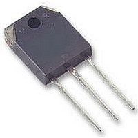
MOSFET N-CH 300V 59A TO-3P
Manufacturer
Fairchild Semiconductor
Series
UniFET™r
Datasheet
1.FDA59N30.pdf
(8 pages)
Specifications of FDA59N30
Fet Type
MOSFET N-Channel, Metal Oxide
Fet Feature
Standard
Rds On (max) @ Id, Vgs
56 mOhm @ 29.5A, 10V
Drain To Source Voltage (vdss)
300V
Current - Continuous Drain (id) @ 25° C
59A
Vgs(th) (max) @ Id
5V @ 250µA
Gate Charge (qg) @ Vgs
100nC @ 10V
Input Capacitance (ciss) @ Vds
4670pF @ 25V
Power - Max
500W
Mounting Type
Through Hole
Package / Case
TO-3PN-3
Transistor Polarity
N Channel
Continuous Drain Current Id
59A
Drain Source Voltage Vds
300V
On Resistance Rds(on)
56mohm
Rds(on) Test Voltage Vgs
10V
Threshold Voltage Vgs Typ
5V
Rohs Compliant
Yes
Configuration
Single
Resistance Drain-source Rds (on)
0.056 Ohms
Drain-source Breakdown Voltage
300 V
Gate-source Breakdown Voltage
+/- 30 V
Continuous Drain Current
59 A
Power Dissipation
500 W
Maximum Operating Temperature
+ 150 C
Mounting Style
Through Hole
Minimum Operating Temperature
- 55 C
Lead Free Status / RoHS Status
Lead free / RoHS Compliant
Available stocks
Company
Part Number
Manufacturer
Quantity
Price
Company:

Part Number:
FDA59N30
Manufacturer:
IDT
Quantity:
1 430
Part Number:
FDA59N30
Manufacturer:
FAIRCHILD/ن»™ç«¥
Quantity:
20 000
Company:
Part Number:
FDA59N30LDTU
Manufacturer:
SAMSUNG
Quantity:
3 023


FDA59N30 Rev. A
Typical Performance Characteristics
Figure 5. Capacitance Characteristics
Figure 3. On-Resistance Variation vs.
Figure 1. On-Region Characteristics
10
10
10
2
1
0
10
9000
6000
3000
-1
Drain Current and Gate Voltage
Top :
Bottom :
0.12
0.11
0.10
0.09
0.08
0.07
0.06
0.05
0.04
0
10
-1
0
10.0 V
15.0 V
5.5 V
8.0 V
7.0 V
6.5 V
6.0 V
V
GS
25
C
C
C
V
oss
iss
rss
DS
V
, Drain-Source Voltage [V]
DS
10
50
, Drain-Source Voltage [V]
0
10
I
D
0
, Drain Current [A]
V
75
GS
= 10V
100
C
C
C
iss
oss
rss
10
= C
= C
125
= C
※
10
1
1. 250µ s Pulse Test
2. T
gs
gd
ds
1
Notes :
※
+ C
+ C
C
Note : T
= 25 ℃
gd
gd
V
※
(C
GS
1. V
2. f = 1 MHz
ds
150
Note ;
= 20V
J
= shorted)
= 25 ℃
GS
= 0 V
175
3
12
10
10
10
10
8
6
4
2
0
10
10
10
2
1
0
0
2
1
0
2
0.2
Figure 2. Transfer Characteristics
Figure 4. Body Diode Forward Voltage
Figure 6. Gate Charge Characteristics
10
0.4
Variation vs. Source Current
25
4
20
150
o
C
150 ℃
0.6
o
Q
C
V
V
G
GS
SD
and Temperatue
, Total Gate Charge [nC]
30
, Source-Drain voltage [V]
, Gate-Source Voltage [V]
25 ℃
0.8
V
6
V
V
DS
DS
DS
40
= 150V
= 240V
-55
= 60V
1.0
o
C
50
8
1.2
60
※
※
1. V
2. 250µ s Pulse Test
1.4
※
Notes :
Note : I
1. V
2. 250µ s Pulse Test
GS
Notes :
70
= 0V
DS
10
D
= 40V
= 59A
1.6
www.fairchildsemi.com
80
1.8
12
Related parts for FDA59N30
Image
Part Number
Description
Manufacturer
Datasheet
Request
R

Part Number:
Description:
Fairchild Semiconductor [IGBT MODULE]
Manufacturer:
Fairchild Semiconductor
Datasheet:

Part Number:
Description:
Discrete Semiconductor Modules
Manufacturer:
Fairchild Semiconductor
Part Number:
Description:
Discrete Semiconductor Modules
Manufacturer:
Fairchild Semiconductor
Part Number:
Description:
This N-Channel MOSFET is produced using Fairchild Semiconductor’s advanced Power Trench® process
Manufacturer:
Fairchild Semiconductor
Datasheet:
Part Number:
Description:
This N-Channel MOSFET is produced using Fairchild Semiconductor’s advanced Power Trench® process
Manufacturer:
Fairchild Semiconductor
Datasheet:
Part Number:
Description:
This N-Channel MOSFET is produced using Fairchild Semiconductor’s advanced PowerTrench® process
Manufacturer:
Fairchild Semiconductor
Datasheet:
Part Number:
Description:
This N-Channel MOSFET is produced using Fairchild Semiconductor’s advanced PowerTrench® process
Manufacturer:
Fairchild Semiconductor
Datasheet:
Part Number:
Description:
This N-Channel MOSFET is produced using Fairchild Semiconductor’s advanced Power Trench® process
Manufacturer:
Fairchild Semiconductor
Datasheet:
Part Number:
Description:
This N-Channel logic Level MOSFETs are produced using Fairchild Semiconductor‘s advanced Power Trench® process that has been special tailored to minimize the on-state resistance and yet maintain superior switching performance
Manufacturer:
Fairchild Semiconductor
Datasheet:
Part Number:
Description:
This N-Channel MOSFET is produced using Fairchild Semiconductor’s advanced Power Trench® process
Manufacturer:
Fairchild Semiconductor
Datasheet:
Part Number:
Description:
This N-Channel SyncFET™ is produced using Fairchild Semiconductor’s advanced PowerTrench® process
Manufacturer:
Fairchild Semiconductor
Datasheet:
Part Number:
Description:
This N-Channel SyncFET™ is produced using Fairchild Semiconductor’s advanced PowerTrench® process
Manufacturer:
Fairchild Semiconductor
Datasheet:
Part Number:
Description:
This N-Channel SyncFET™ is produced using Fairchild Semiconductor’s advanced PowerTrench® process
Manufacturer:
Fairchild Semiconductor
Datasheet:
Part Number:
Description:
This N-Channel logic Level MOSFETs are produced using Fairchild Semiconductor‘s advanced Power Trench® process that has been special tailored to minimize the on-state resistance and yet maintain superior switching performance
Manufacturer:
Fairchild Semiconductor
Datasheet:
Part Number:
Description:
This N-Channel MOSFET is produced using Fairchild Semiconductor’s advanced Power Trench® process that has been especially tailored to minimize the on-state resistance and yet maintain superior switching performance
Manufacturer:
Fairchild Semiconductor
Datasheet: