BSS87,115 NXP Semiconductors, BSS87,115 Datasheet - Page 2
BSS87,115
Manufacturer Part Number
BSS87,115
Description
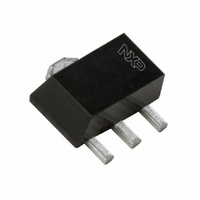
MOSFET N-CH 200V 400MA SOT-89
Manufacturer
NXP Semiconductors
Series
TrenchMOS™r
Type
Power MOSFETr
Datasheet
1.BSS87115.pdf
(8 pages)
Specifications of BSS87,115
Package / Case
SC-62, SOT-89, TO-243 (3 Leads + Tab)
Mounting Type
Surface Mount
Power - Max
1W
Fet Type
MOSFET N-Channel, Metal Oxide
Vgs(th) (max) @ Id
2.8V @ 1mA
Current - Continuous Drain (id) @ 25° C
400mA
Drain To Source Voltage (vdss)
200V
Fet Feature
Standard
Rds On (max) @ Id, Vgs
3 Ohm @ 400mA, 10V
Minimum Operating Temperature
- 55 C
Configuration
Single
Transistor Polarity
N-Channel
Resistance Drain-source Rds (on)
3 Ohm @ 10 V
Drain-source Breakdown Voltage
200 V
Gate-source Breakdown Voltage
+/- 20 V
Continuous Drain Current
0.4 A
Power Dissipation
1000 mW
Maximum Operating Temperature
+ 150 C
Mounting Style
SMD/SMT
Number Of Elements
1
Polarity
N
Channel Mode
Enhancement
Drain-source On-res
3Ohm
Drain-source On-volt
200V
Gate-source Voltage (max)
±20V
Operating Temp Range
-55C to 150C
Operating Temperature Classification
Military
Mounting
Surface Mount
Pin Count
3 +Tab
Package Type
SOT-89
Lead Free Status / RoHS Status
Lead free / RoHS Compliant
Gate Charge (qg) @ Vgs
-
Lead Free Status / Rohs Status
Lead free / RoHS Compliant
Other names
933943940115::BSS87 T/R::BSS87 T/R
Available stocks
Company
Part Number
Manufacturer
Quantity
Price

Part Number:
BSS87,115
Manufacturer:
NEXPERIA/安世
Quantity:
20 000


Philips Semiconductors
FEATURES
APPLICATIONS
DESCRIPTION
N-channel enhancement mode vertical D-MOS transistor
in a SOT89 package.
QUICK REFERENCE DATA
LIMITING VALUES
In accordance with the Absolute Maximum Rating System (IEC 60134).
Note
1. Device mounted on a printed-circuit board, maximum lead length 4 mm; mounting pad for the drain lead minimum
2001 May 18
V
V
I
P
R
V
V
I
I
P
T
T
D
D
DM
y
SYMBOL
SYMBOL
stg
j
Direct interface to C-MOS, TTL, etc.
High-speed switching
No secondary breakdown
Low R
Line current interruptor in telephone sets
Applications in relay, high-speed and line transformer
drivers.
DS
GSO
tot
DS
GSO
tot
DSon
N-channel enhancement mode
vertical D-MOS transistor
fs
10
DSon
10 mm
.
drain-source voltage (DC)
gate-source voltage (DC)
drain current (DC)
total power dissipation
drain-source on-state resistance
forward transfer admittance
drain-source voltage (DC)
gate-source voltage (DC)
drain current (DC)
peak drain current
total power dissipation
storage temperature
junction temperature
PARAMETER
PARAMETER
open drain
T
I
I
open drain
T
D
D
amb
amb
= 400 mA; V
= 400 mA; V
25 C
25 C; note 1
2
CONDITIONS
CONDITIONS
PINNING - SOT89
handbook, halfpage
GS
DS
Fig.1 Simplified outline (SOT89) and symbol.
= 10 V
= 25 V
PIN
Bottom view
1
2
3
1
2
source
drain
gate
140
3
MIN.
55
MIN.
MAM355
DESCRIPTION
1.6
750
TYP.
Product specification
g
200
400
1.6
1
+150
150
20
MAX.
200
400
1
3
MAX.
20
d
s
BSS87
V
V
mA
A
W
C
C
UNIT
V
V
mA
W
mS
UNIT
Related parts for BSS87,115
Image
Part Number
Description
Manufacturer
Datasheet
Request
R

Part Number:
Description:
Intermediate level N-channel enhancement mode Field-Effect Transistor (FET) in a plastic package using vertical D-MOS technology
Manufacturer:
NXP Semiconductors
Datasheet:

Part Number:
Description:
NXP Semiconductors designed the LPC2420/2460 microcontroller around a 16-bit/32-bitARM7TDMI-S CPU core with real-time debug interfaces that include both JTAG andembedded trace
Manufacturer:
NXP Semiconductors
Datasheet:

Part Number:
Description:
NXP Semiconductors designed the LPC2458 microcontroller around a 16-bit/32-bitARM7TDMI-S CPU core with real-time debug interfaces that include both JTAG andembedded trace
Manufacturer:
NXP Semiconductors
Datasheet:
Part Number:
Description:
NXP Semiconductors designed the LPC2468 microcontroller around a 16-bit/32-bitARM7TDMI-S CPU core with real-time debug interfaces that include both JTAG andembedded trace
Manufacturer:
NXP Semiconductors
Datasheet:
Part Number:
Description:
NXP Semiconductors designed the LPC2470 microcontroller, powered by theARM7TDMI-S core, to be a highly integrated microcontroller for a wide range ofapplications that require advanced communications and high quality graphic displays
Manufacturer:
NXP Semiconductors
Datasheet:
Part Number:
Description:
NXP Semiconductors designed the LPC2478 microcontroller, powered by theARM7TDMI-S core, to be a highly integrated microcontroller for a wide range ofapplications that require advanced communications and high quality graphic displays
Manufacturer:
NXP Semiconductors
Datasheet:
Part Number:
Description:
The Philips Semiconductors XA (eXtended Architecture) family of 16-bit single-chip microcontrollers is powerful enough to easily handle the requirements of high performance embedded applications, yet inexpensive enough to compete in the market for hi
Manufacturer:
NXP Semiconductors
Datasheet:
Part Number:
Description:
The XA-S3 device is a member of Philips Semiconductors? XA(eXtended Architecture) family of high performance 16-bitsingle-chip microcontrollers
Manufacturer:
NXP Semiconductors
Datasheet:

Part Number:
Description:
The NXP BlueStreak LH75401/LH75411 family consists of two low-cost 16/32-bit System-on-Chip (SoC) devices
Manufacturer:
NXP Semiconductors
Datasheet:
Part Number:
Description:
The NXP LPC3130/3131 combine an 180 MHz ARM926EJ-S CPU core, high-speed USB2
Manufacturer:
NXP Semiconductors
Datasheet:
Part Number:
Description:
The NXP LPC3141 combine a 270 MHz ARM926EJ-S CPU core, High-speed USB 2
Manufacturer:
NXP Semiconductors
Part Number:
Description:
The NXP LPC3143 combine a 270 MHz ARM926EJ-S CPU core, High-speed USB 2
Manufacturer:
NXP Semiconductors

Part Number:
Description:
The NXP LPC3152 combines an 180 MHz ARM926EJ-S CPU core, High-speed USB 2
Manufacturer:
NXP Semiconductors
Part Number:
Description:
The NXP LPC3154 combines an 180 MHz ARM926EJ-S CPU core, High-speed USB 2
Manufacturer:
NXP Semiconductors