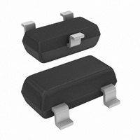
BSH108,215 NXP Semiconductors, BSH108,215 Datasheet - Page 3

BSH108,215
Manufacturer Part Number
BSH108,215
Description
MOSFET N-CH 30V 1.9A SOT23
Manufacturer
NXP Semiconductors
Series
TrenchMOS™r
Datasheet
1.BSH108215.pdf
(13 pages)
Specifications of BSH108,215
Package / Case
SOT-23-3, TO-236-3, Micro3™, SSD3, SST3
Mounting Type
Surface Mount
Power - Max
830mW
Fet Type
MOSFET N-Channel, Metal Oxide
Gate Charge (qg) @ Vgs
10nC @ 10V
Vgs(th) (max) @ Id
2V @ 1mA
Current - Continuous Drain (id) @ 25° C
1.9A
Drain To Source Voltage (vdss)
30V
Fet Feature
Logic Level Gate
Rds On (max) @ Id, Vgs
120 mOhm @ 1A, 10V
Minimum Operating Temperature
- 65 C
Configuration
Single
Transistor Polarity
N-Channel
Resistance Drain-source Rds (on)
0.12 Ohm @ 10 V
Drain-source Breakdown Voltage
30 V
Gate-source Breakdown Voltage
+/- 20 V
Continuous Drain Current
1.9 A
Power Dissipation
830 mW
Maximum Operating Temperature
+ 150 C
Mounting Style
SMD/SMT
Lead Free Status / RoHS Status
Lead free / RoHS Compliant
Lead Free Status / RoHS Status
Lead free / RoHS Compliant, Lead free / RoHS Compliant
Other names
934055571215::BSH108 T/R::BSH108 T/R
Philips Semiconductors
9397 750 07652
Product specification
Fig 1. Normalized total power dissipation as a
Fig 3. Safe operating area; continuous and peak drain currents as a function of drain-source voltage.
T
P
sp
der
= 25 C; I
function of solder point temperature.
P
=
(%)
der
120
100
80
60
40
20
----------------------
P
0
tot 25 C
0
P
tot
DM
25
is single pulse.
100%
50
(A)
I D
75
P
100
t p
T
125
T sp (
=
t p
T
150
t
o
C)
03aa17
175
Rev. 02 — 25 October 2000
N-channel enhancement mode field-effect transistor
Fig 2. Normalized continuous drain current as a
V
I
der
GS
function of solder point temperature.
(%)
=
I der
5 V
------------------ -
I
120
100
D 25 C
80
60
40
20
0
I
D
0
25
100%
50
75
03aa80
© Philips Electronics N.V. 2000. All rights reserved.
100
125
T sp ( o C)
BSH108
150
03aa25
175
3 of 13


