IRLR4343PBF International Rectifier, IRLR4343PBF Datasheet
IRLR4343PBF
Specifications of IRLR4343PBF
Available stocks


Related parts for IRLR4343PBF


IRLR4343PBF Summary of contents
Page 1
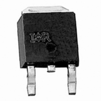
... Notes through Š are on page 10 www.irf.com typ DS(ON) R typ DS(ON) Q typ max J G Parameter @ 10V GS @ 10V GS h Parameter IRLR4343PbF IRLU4343PbF IRLU4343-701PbF Key Parameters 10V 4. 175 °C D D-Pak I-Pak IRLR4343 IRLU4343 I-Pak Leadform 701 IRLU4343-701 S Refer to page 10 for package outline Max. ...
Page 2
Electrical Characteristics @ T Parameter BV Drain-to-Source Breakdown Voltage DSS ∆ΒV /∆T Breakdown Voltage Temp. Coefficient DSS J R Static Drain-to-Source On-Resistance DS(on) V Gate Threshold Voltage GS(th) ∆V /∆T Gate Threshold Voltage Coefficient GS(th Drain-to-Source Leakage Current ...
Page 3
VGS TOP 15V 10V 8.0V 4.5V 100 3.5V 3.0V 2.5V BOTTOM 2.3V 10 2.3V 1 ≤ 60µs PULSE WIDTH Tj = 25°C 0.1 0 Drain-to-Source Voltage (V) Fig 1. Typical Output Characteristics 1000.0 T ...
Page 4
175°C 10.0 1 25° 0.1 0.2 0.4 0.6 0.8 1.0 1.2 1 Source-to-Drain Voltage (V) Fig 7. Typical Source-Drain Diode Forward Voltage ...
Page 5
125° 25°C 0 2.0 4.0 6.0 8 Gate-to-Source Voltage (V) Fig 12. On-Resistance Vs. Gate Voltage 1000 Duty Cycle = Single Pulse 100 0.01 10 0.05 0.10 ...
Page 6
D.U.T + ƒ • • - • + ‚ - R • • • SD • Fig 16. 15V DRIVER D.U 20V GS 0.01 Ω Fig 17a. Unclamped Inductive ...
Page 7
EXAMPLE: T HIS IS AN IRF R120 WIT EMBLY LOT CODE 1234 AS S EMB LED ON WW 16, 1999 EMBLY LINE "A" Note: "P" embly line pos ition ...
Page 8
EXAMPLE: T HIS IS AN IRFU120 WIT EMBLY LOT CODE 5678 AS S EMB 19, 1999 EMBLY LINE "A" Note: "P" embly line pos ition ...
Page 9
TR 12.1 ( .476 ) 11.9 ( .469 ) NOTES : 1. CONTROLLING DIMENSION : MILLIMETER. 2. ALL DIMENSIONS ARE SHOWN IN MILLIMETERS ( INCHES ). 3. OUTLINE CONFORMS TO EIA-481 & EIA-541. 13 INCH NOTES : 1. OUTLINE CONFORMS ...
Page 10
Notes: Repetitive rating; pulse width limited by max. junction temperature. ‚ Starting T = 25° 0.93mH 25Ω 19A ƒ Pulse width ≤ 400µs; duty cycle ≤ 2%. „ This only ...
Page 11
Note: For the most current drawings please refer to the IR website at: http://www.irf.com/package/ ...