STP200NF04L STMicroelectronics, STP200NF04L Datasheet
STP200NF04L
Specifications of STP200NF04L
Available stocks


Related parts for STP200NF04L


STP200NF04L Summary of contents
Page 1
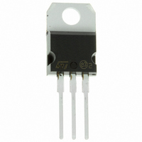
... April 2005 STB200NF04L - STB200NF04L-1 Figure 1: Package R I DS(on) D 3.5 m 120 A 3.8 m 120 A 3.8 m 120 A Figure 2: Internal Schematic Diagram MARKING PACKAGE P200NF04L TO-220 B200NF04L D²PAK B200NF04L I²PAK STP200NF04L STripFET™ II MOSFET TO-220 I²PAK PACKAGING TUBE TAPE & REEL TUBE Rev D²PAK 1/12 ...
Page 2
... STP200NF04L - STB200NF04L - STB200NF04L-1 Table 3: Absolute Maximum ratings Symbol V Drain-source Voltage ( Drain-gate Voltage (R GDR V Gate- source Voltage GS I (**) Drain Current (continuous Drain Current (continuous (2) Drain Current (pulsed Total Dissipation at T TOT Derating Factor Peak Diode Recovery voltage slope dv/dt (1) E (3) Single Pulse Avalanche Energy ...
Page 3
... I (1) Source-drain Current (pulsed) SDM V (4) Forward On Voltage SD t Reverse Recovery Time rr Q Reverse Recovery Charge rr Reverse Recovery Current I RRM (1) Pulse width limited by safe operating area (4). Pulsed: Pulse duration = 300 µs, duty cycle 1.5 %. STP200NF04L - STB200NF04L - STB200NF04L-1 Test Conditions 25V MHz ...
Page 4
... STP200NF04L - STB200NF04L - STB200NF04L-1 Figure 3: Safe Operating Area Figure 4: Output Characteristics Figure 5: Transconductance 4/12 Figure 6: Thermal Impedance Figure 7: Transfer Characteristics Figure 8: Static Drain-source On Resistance ...
Page 5
... Figure 9: Gate Charge vs Gate-source Voltage Figure 10: Normalized Gate Thereshold Volt- age vs Temperature Figure 11: Source-Drain Diode Forward Char- acteristics STP200NF04L - STB200NF04L - STB200NF04L-1 Figure 12: Capacitance Variations Figure 13: Normalized On Resistance vs Tem- perature Figure 14: Normalized Breakdown Voltage vs Temperature 5/12 ...
Page 6
... STP200NF04L - STB200NF04L - STB200NF04L-1 Figure 15: Unclamped Inductive Load Test Cir- cuit Figure 16: Switching Times Test Circuit For Resistive Load Figure 17: Test Circuit For Inductive Load Switching and Diode Recovery Times 6/12 Figure 18: Unclamped Inductive Wafeform Figure 19: Gate Charge Test Circuit ...
Page 7
... D 15. 2.40 e1 4.95 F 1.23 H1 6. 3.50 L20 16.40 L30 28.90 øP 3.75 Q 2.65 STP200NF04L - STB200NF04L - STB200NF04L-1 mm. TYP MAX. 4.60 0.173 0.88 0.024 1.70 0.045 0.70 0.019 15.75 10.40 0.393 2.70 0.094 5.15 0.194 1.32 0.048 6.60 0.244 2.72 0.094 14 0.511 3 ...
Page 8
... STP200NF04L - STB200NF04L - STB200NF04L-1 DIM. MIN. A 4.40 A1 2.40 b 0.61 b1 1.14 c 0.49 c2 1.23 D 8.95 e 2. 3.50 L2 1.27 8/12 2 TO-262 (I PAK) MECHANICAL DATA mm. TYP MAX. MIN. 4.60 0.173 2.72 0.094 0.88 0.024 1.70 0.044 0.70 0.019 1.32 0.048 9.35 0.352 2.70 0.094 5.15 ...
Page 9
... C 0.45 C2 1. 8 1.27 L3 1.4 M 2.4 R 0.4 V2 0º STP200NF04L - STB200NF04L - STB200NF04L-1 MAX. MIN. 4.6 0.173 2.69 0.098 0.23 0.001 0.93 0.027 1.7 0.044 0.6 0.017 1.36 0.048 9.35 0.352 10.4 0.393 5.28 0.192 15.85 0.590 1.4 0.050 1 ...
Page 10
... STP200NF04L - STB200NF04L - STB200NF04L PAK FOOTPRINT TAPE MECHANICAL DATA mm DIM. MIN. MAX. A0 10.5 10.7 B0 15.7 15.9 D 1.5 1.6 D1 1.59 1.61 E 1.65 1.85 F 11.4 11.6 K0 4.8 5.0 P0 3.9 4.1 P1 11.9 12.1 P2 1.9 2 0.25 0.35 0.0098 0.0137 W 23.7 24 sales type 10/12 TAPE AND REEL SHIPMENT inch MIN ...
Page 11
... Table 8: Revision History Date Revision 11/Apr/2005 1 STP200NF04L - STB200NF04L - STB200NF04L-1 Description of Changes First Release. 11/12 ...
Page 12
... STP200NF04L - STB200NF04L - STB200NF04L-1 Information furnished is believed to be accurate and reliable. However, STMicroelectronics assumes no responsibility for the consequences of use of such information nor for any infringement of patents or other rights of third parties which may result from its use. No license is granted by implication or otherwise under any patent or patent rights of STMicroelectronics. Specifications mentioned in this publication are subject to change without notice ...