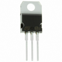
STP200NF04L STMicroelectronics, STP200NF04L Datasheet - Page 2

STP200NF04L
Manufacturer Part Number
STP200NF04L
Description
MOSFET N-CH 40V 120A TO-220
Manufacturer
STMicroelectronics
Series
STripFET™r
Datasheet
1.STB200NF04L.pdf
(12 pages)
Specifications of STP200NF04L
Fet Type
MOSFET N-Channel, Metal Oxide
Fet Feature
Logic Level Gate
Rds On (max) @ Id, Vgs
3.8 mOhm @ 50A, 10V
Drain To Source Voltage (vdss)
40V
Current - Continuous Drain (id) @ 25° C
120A
Vgs(th) (max) @ Id
4V @ 250µA
Gate Charge (qg) @ Vgs
90nC @ 4.5V
Input Capacitance (ciss) @ Vds
6400pF @ 25V
Power - Max
300W
Mounting Type
Through Hole
Package / Case
TO-220-3 (Straight Leads)
Configuration
Single
Transistor Polarity
N-Channel
Resistance Drain-source Rds (on)
3 m Ohms
Forward Transconductance Gfs (max / Min)
60 S
Drain-source Breakdown Voltage
40 V
Gate-source Breakdown Voltage
+/- 16 V
Continuous Drain Current
120 A
Power Dissipation
300 W
Maximum Operating Temperature
+ 175 C
Mounting Style
Through Hole
Fall Time
80 ns
Minimum Operating Temperature
- 55 C
Rise Time
270 ns
Lead Free Status / RoHS Status
Lead free / RoHS Compliant
Other names
497-4819-5
Available stocks
Company
Part Number
Manufacturer
Quantity
Price
Company:
Part Number:
STP200NF04L
Manufacturer:
ST
Quantity:
25 000
Company:
Part Number:
STP200NF04L
Manufacturer:
ST
Quantity:
12 500
Part Number:
STP200NF04L
Manufacturer:
RUICHIPS
Quantity:
20 000
STP200NF04L - STB200NF04L - STB200NF04L-1
2/12
Table 3: Absolute Maximum ratings
(1)I
(2) Pulse width limited by safe operating area.
(3) Starting T
(**) Current limited by Package
Table 4: Thermal Data
(*)When mounted on 1 inch² FR4 2oZ Cu
ELECTRICAL CHARACTERISTICS (T
Table 5: On/Off
Rthj-pcb (*)
Rthj-case
V
SD
Symbol
Symbol
dv/dt (1)
R
E
V
I
(BR)DSS
I
V
DM
P
Rthja
D
I
I
DS(on)
V
V
AS
GS(th)
T
DSS
GSS
GDR
TOT
I
T
T
DS
GS
stg
(**)
D
100 A, di/dt
j
l
(2)
(3)
j
= 25°C, I
Drain-source
Breakdown Voltage
Zero Gate Voltage
Drain Current (V
Gate-body Leakage
Current (V
Gate Threshold Voltage V
Static Drain-source On
Resistance
Drain-source Voltage (V
Drain-gate Voltage (R
Gate- source Voltage
Drain Current (continuous) at T
Drain Current (continuous) at T
Drain Current (pulsed)
Total Dissipation at T
Derating Factor
Peak Diode Recovery voltage slope
Single Pulse Avalanche Energy
Storage Temperature
Max. Operating Junction Temperature
Thermal Resistance Junction-case
Thermal Resistance Junction-pcb
Thermal Resistance Junction-ambient
Maximum Lead Temperature For Soldering Purpose
240 A/µs, V
AR
Parameter
= 50A, V
DS
DD
= 0)
DD
GS
= 30V
32 , T
= 0)
C
GS
Parameter
j
= 25°C
GS
=20 K
T
I
V
V
V
V
V
V
V
D
JMAX
DS
D
GS
DS
GS
GS
GS
GS
= 0)
= 250 µA, V
= Max Rating, T
CASE
= Max Rating
= V
= ± 16V
= 10 V, I
= 5 V, I
= 10 V, I
= 5 V, I
C
C
Test Conditions
= 25°C
= 100°C
GS
=25°C UNLESS OTHERWISE SPECIFIED)
, I
D
D
D
D
D
GS
= 250µA
= 50 A
= 50 A
= 50 A
= 50 A
= 0
C
Max
Max
Max
= 125 °C
TO-220
I²PAK
D²PAK
TO-220/I²PAK
62.5
300
Min.
40
1
-55 to 175
Value
± 16
120
120
480
300
1.4
0.50
3.6
40
40
2
Typ.
3.3
3.8
3.0
3.5
D²PAK
35
--
--
±100
Max.
3.8
4.6
3.5
4.3
10
1
4
W/°C
°C/W
°C/W
V/ns
Unit
Unit
Unit
m
m
m
m
µA
µA
nA
°C
°C
W
V
V
V
A
A
A
V
V
J


