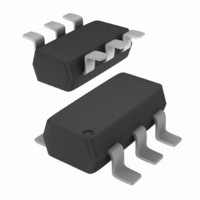
NTGS4111PT1G ON Semiconductor, NTGS4111PT1G Datasheet

MOSFET P-CH 30V 2.6A 6-TSOP

NTGS4111PT1G

Manufacturer Part Number
NTGS4111PT1G
Description
MOSFET P-CH 30V 2.6A 6-TSOP
Manufacturer
ON Semiconductor
Type
Power MOSFETr
Datasheet

Specifications of NTGS4111PT1G

Fet Type
MOSFET P-Channel, Metal Oxide
Fet Feature
Logic Level Gate
Rds On (max) @ Id, Vgs
60 mOhm @ 3.7A, 10V
Drain To Source Voltage (vdss)
30V
Current - Continuous Drain (id) @ 25° C
2.6A
Vgs(th) (max) @ Id
3V @ 250µA
Gate Charge (qg) @ Vgs
32nC @ 10V
Input Capacitance (ciss) @ Vds
750pF @ 15V
Power - Max
630mW
Mounting Type
Surface Mount
Package / Case
SC-74-6
Configuration
Single Quad Drain
Transistor Polarity
P-Channel
Resistance Drain-source Rds (on)
0.06 Ohm @ 10 V
Forward Transconductance Gfs (max / Min)
6 S
Drain-source Breakdown Voltage
30 V
Gate-source Breakdown Voltage
+/- 20 V
Continuous Drain Current
3.7 A
Power Dissipation
1250 mW
Maximum Operating Temperature
+ 150 C
Mounting Style
SMD/SMT
Minimum Operating Temperature
- 55 C
Number Of Elements
1
Polarity
P
Channel Mode
Enhancement
Drain-source On-res
0.06Ohm
Drain-source On-volt
30V
Gate-source Voltage (max)
±20V
Operating Temp Range
-55C to 150C
Operating Temperature Classification
Military
Mounting
Surface Mount
Pin Count
6
Package Type
TSOP
Dc
04+
Lead Free Status / RoHS Status
Lead free / RoHS Compliant
Other names
NTGS4111PT1GOSTR

Available stocks

Company
Part Number
Manufacturer
Quantity
Price
Part Number:
NTGS4111PT1G
Manufacturer:
ST
Quantity:
30 000
Part Number:
NTGS4111PT1G
Manufacturer:
ON
Quantity:
48 000
Part Number:
NTGS4111PT1G
Manufacturer:
ON
Quantity:
30 000
Part Number:
NTGS4111PT1G
Manufacturer:
ON/安森美
Quantity:
20 000
Part Number:
NTGS4111PT1G
0
Company:
Part Number:
NTGS4111PT1G
Quantity:
24 000
NTGS4111P
Power MOSFET
−30 V, −4.7 A, Single P−Channel, TSOP−6
Features
Applications
Stresses exceeding Maximum Ratings may damage the device. Maximum
Ratings are stress ratings only. Functional operation above the Recommended
Operating Conditions is not implied. Extended exposure to stresses above the
Recommended Operating Conditions may affect device reliability.
1. Surface−mounted on FR4 board using 1 in sq pad size
2. Surface−mounted on FR4 board using the minimum recommended pad size
© Semiconductor Components Industries, LLC, 2009
July, 2009 − Rev. 3
MAXIMUM RATINGS
THERMAL RESISTANCE RATINGS
Drain−to−Source Voltage
Gate−to−Source Voltage
Continuous Drain
Current (Note 1)
Power Dissipation
(Note 1)
Continuous Drain
Current (Note 2)
Power Dissipation
(Note 2)
Pulsed Drain Current
Operating Junction and Storage Temperature
Source Current (Body Diode)
Lead Temperature for Soldering Purposes
(1/8″ from case for 10 s)
Junction−to−Ambient – Steady State (Note 1)
Junction−to−Ambient – t ≤ 5 s (Note 1)
Junction−to−Ambient – Steady State (Note 2)
Leading −30 V Trench Process for Low R
Low Profile Package Suitable for Portable Applications
Surface Mount TSOP−6 Package Saves Board Space
Improved Efficiency for Battery Applications
Pb−Free Package is Available
Battery Management and Switching
Load Switching
Battery Protection
(Cu area = 1.127 in sq [1 oz] including traces).
(Cu area = 0.006 in sq).
Rating
Rating
(T
J
Steady
Steady
Steady
t ≤ 5 s
t ≤ 5 s
= 25°C unless otherwise noted)
State
State
State
tp = 10 ms
T
T
T
T
T
T
T
A
A
A
A
A
A
A
= 25°C
= 85°C
= 25°C
= 25°C
= 25°C
= 85°C
= 25°C
DS(on)
Symbol
Symbol
R
R
R
V
T
V
I
P
P
T
DSS
STG
T
qJA
qJA
qJA
DM
I
I
I
GS
D
D
S
J
D
D
L
,
−55 to
Value
−3.7
−2.7
−4.7
1.25
−2.6
−1.9
0.63
−1.7
Max
62.5
−30
±20
−15
150
260
100
200
2.0
1
°C/W
Unit
Unit
°C
°C
W
W
V
V
A
A
A
A
NTGS4111PT1
NTGS4111PT1G
†For information on tape and reel specifications,
including part orientation and tape sizes, please
refer to our Tape and Reel Packaging Specifications
Brochure, BRD8011/D.
V
CASE 318G
*Date Code orientation may vary depending
(BR)DSS
−30 V
STYLE 1
upon manufacturing location.
TSOP−6
Device
(Note: Microdot may be in either location)
TG
M
G
ORDERING INFORMATION
1
3
http://onsemi.com
68 mW @ −4.5 V
38 mW @ −10 V
= Specific Device Code
= Date Code*
= Pb−Free Package
(Pb−Free)
R
Package
TSOP−6
TSOP−6
DS(on)
MARKING DIAGRAM &
P−Channel
4
PIN ASSIGNMENT
Publication Order Number:
1 2 5 6
Drain
Drain
TYP
6
1
TG M G
3000 / Tape & Reel
3000 / Tape& Reel
Drain
Drain
G
5
2
Shipping
NTGS4111P/D
Source
4
3
Gate
I
D
−4.7 A
MAX

Related parts for NTGS4111PT1G

NTGS4111PT1G Summary of contents

Page 1

... Max Unit °C/W R 100 qJA 62.5 R Device qJA R 200 qJA NTGS4111PT1 NTGS4111PT1G †For information on tape and reel specifications, including part orientation and tape sizes, please refer to our Tape and Reel Packaging Specifications Brochure, BRD8011/D. 1 http://onsemi.com R TYP I MAX D DS(on −10 V −4 − ...

Page 2

ELECTRICAL CHARACTERISTICS Characteristic OFF CHARACTERISTICS Drain−to−Source Breakdown Voltage Drain−to−Source Breakdown Voltage Temperature Coefficient Zero Gate Voltage Drain Current Gate−to−Source Leakage Current ON CHARACTERISTICS (Note 3) Gate Threshold Voltage Negative Threshold Temperature Coefficient Drain−to−Source On Resistance Forward Transconductance CHARGES, CAPACITANCES AND ...

Page 3

TYPICAL PERFORMANCE CURVES 12 −4.5 V −4.2 V −10V 11 10 − − −5 − 25° 0.4 0.8 1.2 1.6 2 2.4 ...

Page 4

TYPICAL PERFORMANCE CURVES 1400 C iss 1300 1200 C rss 1100 1000 900 800 700 600 500 400 300 C oss 200 100 rss ...

Page 5

... Pb−Free strategy and soldering details, please download the ON Semiconductor Soldering and Mounting Techniques Reference Manual, SOLDERRM/D. ON Semiconductor and are registered trademarks of Semiconductor Components Industries, LLC (SCILLC). SCILLC reserves the right to make changes without further notice to any products herein ...

Related keywords