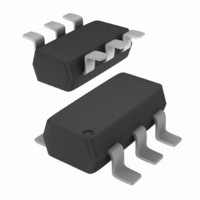
NTGS4111PT1G ON Semiconductor, NTGS4111PT1G Datasheet - Page 4

NTGS4111PT1G
Manufacturer Part Number
NTGS4111PT1G
Description
MOSFET P-CH 30V 2.6A 6-TSOP
Manufacturer
ON Semiconductor
Type
Power MOSFETr
Datasheet
1.NTGS4111PT1G.pdf
(5 pages)
Specifications of NTGS4111PT1G
Fet Type
MOSFET P-Channel, Metal Oxide
Fet Feature
Logic Level Gate
Rds On (max) @ Id, Vgs
60 mOhm @ 3.7A, 10V
Drain To Source Voltage (vdss)
30V
Current - Continuous Drain (id) @ 25° C
2.6A
Vgs(th) (max) @ Id
3V @ 250µA
Gate Charge (qg) @ Vgs
32nC @ 10V
Input Capacitance (ciss) @ Vds
750pF @ 15V
Power - Max
630mW
Mounting Type
Surface Mount
Package / Case
SC-74-6
Configuration
Single Quad Drain
Transistor Polarity
P-Channel
Resistance Drain-source Rds (on)
0.06 Ohm @ 10 V
Forward Transconductance Gfs (max / Min)
6 S
Drain-source Breakdown Voltage
30 V
Gate-source Breakdown Voltage
+/- 20 V
Continuous Drain Current
3.7 A
Power Dissipation
1250 mW
Maximum Operating Temperature
+ 150 C
Mounting Style
SMD/SMT
Minimum Operating Temperature
- 55 C
Number Of Elements
1
Polarity
P
Channel Mode
Enhancement
Drain-source On-res
0.06Ohm
Drain-source On-volt
30V
Gate-source Voltage (max)
±20V
Operating Temp Range
-55C to 150C
Operating Temperature Classification
Military
Mounting
Surface Mount
Pin Count
6
Package Type
TSOP
Dc
04+
Lead Free Status / RoHS Status
Lead free / RoHS Compliant
Other names
NTGS4111PT1GOSTR
Available stocks
Company
Part Number
Manufacturer
Quantity
Price
Company:
Part Number:
NTGS4111PT1G
Manufacturer:
ST
Quantity:
30 000
Company:
Part Number:
NTGS4111PT1G
Manufacturer:
ON
Quantity:
48 000
Company:
Part Number:
NTGS4111PT1G
Manufacturer:
ON
Quantity:
30 000
Part Number:
NTGS4111PT1G
Manufacturer:
ON/安森美
Quantity:
20 000
−GATE−TO−SOURCE OR DRAIN−TO−SOURCE VOLTAGE (VOLTS)
0.01
0.0001
1400
1300
1200
1000
1100
100
0.1
0.001
900
800
700
600
500
400
300
200
100
10
0.01
1
0.1
0.1
0
1E−07
10
1
V
SINGLE PULSE
T
Figure 9. Maximum Rated Forward Biased
C
C
GS
C
V
−V
D = 0.5
iss
rss
0.05
0.02
0.01
0.1
= 25°C
0.2
DS
Single Pulse
= −20 V
DS
5
= 0 V
−V
, DRAIN−TO−SOURCE VOLTAGE (VOLTS)
1E−06
GS
Figure 7. Capacitance Variation
R
THERMAL LIMIT
PACKAGE LIMIT
0
DS(on)
Safe Operating Area
V
−V
GS
1
DS
TYPICAL PERFORMANCE CURVES
= 0 V
LIMIT
5
1E−05
C
oss
10
C
rss
15
1E−04
10
Figure 11. FET Thermal Response
20
T
100 ms
J
1 ms
10 ms
dc
1E−03
= 25°C
25
http://onsemi.com
C
iss
100
30
t, TIME (s)
4
1E−02
12
10
8
6
4
2
0
0
0.1
10
(T
1
Q
1
0.3
J
Figure 8. Gate−to−Source Voltage vs. Total
GS
= 25°C unless otherwise noted)
2
V
Figure 10. Diode Forward Voltage vs. Current
V
DS
1E−01
GS
−V
3
0.4
SD
= 0 V
Q
4
Q
g
, SOURCE−TO−DRAIN VOLTAGE (VOLTS)
, TOTAL GATE CHARGE (nC)
GD
5
0.5
T
J
6
= 150°C
1E+00
Gate Charge
7
0.6
QT
8
9
0.7
1E+01
10
11
V
0.8
GS
12
T
J
I
T
13
D
= −55°C
J
0.9
1E+02
T
= −3.7 A
= 25°C
J
14
T
= 25°C
J
= 100°C
15
1.0
16
1E+03
20
10
0
1.1


