NDF08N50ZG ON Semiconductor, NDF08N50ZG Datasheet - Page 6
NDF08N50ZG
Manufacturer Part Number
NDF08N50ZG
Description
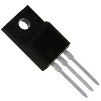
MOSFET N-CH 500V 7.5A TO-220FP
Manufacturer
ON Semiconductor
Datasheet
1.NDF08N50ZG.pdf
(6 pages)
Specifications of NDF08N50ZG
Package / Case
TO-220-3 Full Pack (Straight Leads)
Mounting Type
Through Hole
Power - Max
31W
Fet Type
MOSFET N-Channel, Metal Oxide
Gate Charge (qg) @ Vgs
31nC @ 10V
Vgs(th) (max) @ Id
4.5V @ 100µA
Current - Continuous Drain (id) @ 25° C
7.5A
Drain To Source Voltage (vdss)
500V
Fet Feature
Standard
Rds On (max) @ Id, Vgs
850 mOhm @ 3.6A, 10V
Configuration
Single
Transistor Polarity
N-Channel
Resistance Drain-source Rds (on)
0.69 Ohms
Forward Transconductance Gfs (max / Min)
6 S
Drain-source Breakdown Voltage
500 V
Gate-source Breakdown Voltage
30 V
Continuous Drain Current
4.7 A
Power Dissipation
31 W
Maximum Operating Temperature
+ 125 C
Mounting Style
Through Hole
Gate Charge Qg
31 nC
Minimum Operating Temperature
- 55 C
Lead Free Status / RoHS Status
Lead free / RoHS Compliant
Available stocks
Company
Part Number
Manufacturer
Quantity
Price
Company:

Part Number:
NDF08N50ZG
Manufacturer:
ON
Quantity:
5 950
Company:
Part Number:
NDF08N50ZG
Manufacturer:
ON Semiconductor
Quantity:
5


PUBLICATION ORDERING INFORMATION
LITERATURE FULFILLMENT:
Literature Distribution Center for ON Semiconductor
P.O. Box 5163, Denver, Colorado 80217 USA
Phone: 303−675−2175 or 800−344−3860 Toll Free USA/Canada
Fax: 303−675−2176 or 800−344−3867 Toll Free USA/Canada
Email: orderlit@onsemi.com
ON Semiconductor and
to any products herein. SCILLC makes no warranty, representation or guarantee regarding the suitability of its products for any particular purpose, nor does SCILLC assume any liability
arising out of the application or use of any product or circuit, and specifically disclaims any and all liability, including without limitation special, consequential or incidental damages.
“Typical” parameters which may be provided in SCILLC data sheets and/or specifications can and do vary in different applications and actual performance may vary over time. All
operating parameters, including “Typicals” must be validated for each customer application by customer’s technical experts. SCILLC does not convey any license under its patent rights
nor the rights of others. SCILLC products are not designed, intended, or authorized for use as components in systems intended for surgical implant into the body, or other applications
intended to support or sustain life, or for any other application in which the failure of the SCILLC product could create a situation where personal injury or death may occur. Should
Buyer purchase or use SCILLC products for any such unintended or unauthorized application, Buyer shall indemnify and hold SCILLC and its officers, employees, subsidiaries, affiliates,
and distributors harmless against all claims, costs, damages, and expenses, and reasonable attorney fees arising out of, directly or indirectly, any claim of personal injury or death
associated with such unintended or unauthorized use, even if such claim alleges that SCILLC was negligent regarding the design or manufacture of the part. SCILLC is an Equal
Opportunity/Affirmative Action Employer. This literature is subject to all applicable copyright laws and is not for resale in any manner.
H
Q
Z
A
K
F
L
V
G
Q
H
1 2 3
4
are registered trademarks of Semiconductor Components Industries, LLC (SCILLC). SCILLC reserves the right to make changes without further notice
1 2 3
B
−B−
N
D
0.25 (0.010)
D
3 PL
G
N
L
A
K
−Y−
F
M
B
M
T
U
U
N. American Technical Support: 800−282−9855 Toll Free
Europe, Middle East and Africa Technical Support:
Japan Customer Focus Center
PACKAGE DIMENSIONS
USA/Canada
Phone: 421 33 790 2910
Phone: 81−3−5773−3850
Y
R
J
C
S
TO−220 FULLPAK
http://onsemi.com
CASE 221D−03
CASE 221A−09
−T−
J
C
ISSUE AF
ISSUE K
S
R
TO−220
SEATING
PLANE
−T−
6
SEATING
PLANE
NOTES:
1. DIMENSIONING AND TOLERANCING PER ANSI
2. CONTROLLING DIMENSION: INCH
3. 221D-01 THRU 221D-02 OBSOLETE, NEW
Y14.5M, 1982.
STANDARD 221D-03.
STYLE 1:
DIM
NOTES:
A
B
C
D
G
H
K
N
Q
R
S
U
F
J
L
1. DIMENSIONING AND TOLERANCING PER ANSI
2. CONTROLLING DIMENSION: INCH.
3. DIMENSION Z DEFINES A ZONE WHERE ALL
PIN 1. GATE
Y14.5M, 1982.
BODY AND LEAD IRREGULARITIES ARE
ALLOWED.
STYLE 5:
2. DRAIN
3. SOURCE
DIM
0.617
0.392
0.177
0.024
0.018
0.503
0.048
0.122
0.099
0.092
0.239
0.116
0.118
MIN
A
B
C
D
G
H
K
N
Q
R
S
U
V
F
J
L
T
Z
PIN 1. GATE
0.100 BSC
0.200 BSC
INCHES
2. DRAIN
3. SOURCE
4. DRAIN
0.570
0.380
0.160
0.025
0.142
0.095
0.110
0.014
0.500
0.045
0.190
0.100
0.080
0.045
0.235
0.000
0.045
MIN
---
0.635
0.419
0.193
0.039
0.129
0.135
0.025
0.541
0.058
0.138
0.271
0.117
0.113
MAX
INCHES
ON Semiconductor Website: www.onsemi.com
Order Literature: http://www.onsemi.com/orderlit
For additional information, please contact your local
Sales Representative
0.620
0.405
0.190
0.035
0.161
0.105
0.155
0.025
0.562
0.060
0.210
0.120
0.055
0.255
0.050
0.080
0.110
MAX
---
15.67
12.78
MILLIMETERS
MIN
9.96
4.50
0.60
2.95
3.00
0.45
1.23
3.10
2.51
2.34
6.06
2.54 BSC
5.08 BSC
14.48
12.70
MILLIMETERS
MIN
9.66
4.07
0.64
3.61
2.42
2.80
0.36
1.15
4.83
2.54
2.04
1.15
5.97
0.00
1.15
---
16.12
10.63
13.73
MAX
4.90
1.00
3.28
3.43
0.63
1.47
3.50
2.96
2.87
6.88
MAX
15.75
10.28
14.27
4.82
0.88
4.09
2.66
3.93
0.64
1.52
5.33
3.04
2.79
1.39
6.47
1.27
2.04
---
NDF08N50Z/D
Related parts for NDF08N50ZG
Image
Part Number
Description
Manufacturer
Datasheet
Request
R

Part Number:
Description:
ON Semiconductor [VOLTAGE REGULATOR]
Manufacturer:
ON Semiconductor
Datasheet:
Part Number:
Description:
357-036-542-201 CARDEDGE 36POS DL .156 BLK LOPRO
Manufacturer:
ON Semiconductor
Datasheet:
Part Number:
Description:
357-036-542-201 CARDEDGE 36POS DL .156 BLK LOPRO
Manufacturer:
ON Semiconductor
Datasheet:
Part Number:
Description:
357-036-542-201 CARDEDGE 36POS DL .156 BLK LOPRO
Manufacturer:
ON Semiconductor
Datasheet:
Part Number:
Description:
357-036-542-201 CARDEDGE 36POS DL .156 BLK LOPRO
Manufacturer:
ON Semiconductor
Datasheet:
Part Number:
Description:
357-036-542-201 CARDEDGE 36POS DL .156 BLK LOPRO
Manufacturer:
ON Semiconductor
Datasheet:
Part Number:
Description:
357-036-542-201 CARDEDGE 36POS DL .156 BLK LOPRO
Manufacturer:
ON Semiconductor
Datasheet:
Part Number:
Description:
357-036-542-201 CARDEDGE 36POS DL .156 BLK LOPRO
Manufacturer:
ON Semiconductor
Datasheet:
Part Number:
Description:
357-036-542-201 CARDEDGE 36POS DL .156 BLK LOPRO
Manufacturer:
ON Semiconductor
Datasheet:
Part Number:
Description:
357-036-542-201 CARDEDGE 36POS DL .156 BLK LOPRO
Manufacturer:
ON Semiconductor
Datasheet:
Part Number:
Description:
357-036-542-201 CARDEDGE 36POS DL .156 BLK LOPRO
Manufacturer:
ON Semiconductor
Datasheet:
Part Number:
Description:
Manufacturer:
ON Semiconductor
Datasheet:
Part Number:
Description:
Manufacturer:
ON Semiconductor
Datasheet:
Part Number:
Description:
Manufacturer:
ON Semiconductor
Datasheet: