IPP041N12N3 G Infineon Technologies, IPP041N12N3 G Datasheet
IPP041N12N3 G
Specifications of IPP041N12N3 G


Related parts for IPP041N12N3 G

IPP041N12N3 G Summary of contents
Page 1
... IPI041N12N3 G IPP041N12N3 G PG-TO262-3 PG-TO220-3 041N12N 041N12N Symbol Conditions =25 ° =100 ° =25 °C D,pulse =100 =25 °C tot stg page 1 IPI041N12N3 G IPP041N12N3 G IPB038N12N3 G 120 3.8 120 Value Unit 120 A 120 480 900 mJ ±20 V 300 W -55 ... 175 °C 55/175/ 2009-07-16 ...
Page 2
... Current is limited by bondwire; with See figure =150 °C and duty cycle D=0.01 for V jmax 5) Device 1.5 mm epoxy PCB FR4 with 6 cm connection. PCB is vertical in still air. Rev. 2.2 IPP041N12N3 G Symbol Conditions R thJC R minimal footprint thJA cooling area =25 °C, unless otherwise specified ...
Page 3
... MHz C rss t d( =100 d(off =60 =100 plateau Q V =60 oss =25 ° S,pulse =100 =25 ° = /dt =100 A/µ page 3 IPI041N12N3 G IPP041N12N3 G IPB038N12N3 G Values min. typ. max. - 10400 13800 pF - 1320 1760 - 52 158 211 - 5 182 243 - - 120 - - 480 - 0.9 1.2 - 123 - 356 - Unit 2009-07-16 ...
Page 4
... Drain current I =f 140 120 100 100 150 200 0 [° Max. transient thermal impedance Z =f(t thJC p parameter µs 100 µs 10 µ [V] DS page 4 IPI041N12N3 G IPP041N12N3 G IPB038N12N3 G ≥ 100 150 T [° 0.5 0.2 0.1 0.05 0.02 0.01 single pulse - [s] p 200 0 10 2009-07-16 ...
Page 5
... DS(on)max parameter 300 250 200 150 100 175 ° Rev. 2.2 6 Typ. drain-source on resistance R =f(I DS(on) parameter [ Typ. forward transconductance g =f 200 160 120 80 25 ° [V] GS page 5 IPI041N12N3 G IPP041N12N3 G IPB038N12N3 =25 ° 4 5 100 I [A] D =25 ° 100 I [ 150 150 2009-07-16 ...
Page 6
... I 4 3.5 3 2.5 2 typ 1 100 140 180 -60 [° Forward characteristics of reverse diode I =f parameter 100 0 [V] DS page 6 IPI041N12N3 G IPP041N12N3 G IPB038N12N3 2700 µA 270 µA - 100 140 T [° 175 °C, 98% 25 °C 175 °C 25 °C, 98% 0.5 1 1.5 V [V] SD 180 2 2009-07-16 ...
Page 7
... T Rev. 2.2 14 Typ. gate charge V =f(Q GS parameter °C 6 100 °C 4 150 ° 100 1000 [µ Gate charge waveforms s(th) Q g(th) 60 100 140 180 [°C] j page 7 IPI041N12N3 G IPP041N12N3 G IPB038N12N3 =100 A pulsed gate 100 150 Q [nC] gate 200 Q g ate 2009-07-16 ...
Page 8
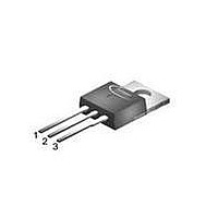
... PG-TO220-3: Outline Rev. 2.2 IPP041N12N3 G page 8 IPI041N12N3 G IPB038N12N3 G 2009-07-16 ...
Page 9
... Rev. 2.2 IPP041N12N3 G page 9 IPI041N12N3 G IPB038N12N3 G 2009-07-16 ...
Page 10
... PG-TO-263 (D²-Pak) Rev. 2.2 IPP041N12N3 G page 10 IPI041N12N3 G IPB038N12N3 G 2009-07-16 ...
Page 11
... Life support devices or systems are intended to be implanted in the human body support and/or maintain and sustain and/or protect human life. If they fail reasonable to assume that the health of the user or other persons may be endangered. Rev. 2.2 IPP041N12N3 G ). page 11 IPI041N12N3 G IPB038N12N3 G ...