IRLR8503 International Rectifier, IRLR8503 Datasheet - Page 2
IRLR8503
Manufacturer Part Number
IRLR8503
Description
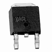
MOSFET N-CH 30V 44A DPAK
Manufacturer
International Rectifier
Series
HEXFET®r
Datasheet
1.IRLR8503.pdf
(9 pages)
Specifications of IRLR8503
Fet Type
MOSFET N-Channel, Metal Oxide
Fet Feature
Logic Level Gate
Rds On (max) @ Id, Vgs
16 mOhm @ 15A, 10V
Drain To Source Voltage (vdss)
30V
Current - Continuous Drain (id) @ 25° C
44A
Vgs(th) (max) @ Id
3V @ 250µA
Gate Charge (qg) @ Vgs
20nC @ 5V
Input Capacitance (ciss) @ Vds
1650pF @ 25V
Power - Max
62W
Mounting Type
Surface Mount
Package / Case
DPak, TO-252 (2 leads+tab), SC-63
Lead Free Status / RoHS Status
Contains lead / RoHS non-compliant
Other names
*IRLR8503
Available stocks
Company
Part Number
Manufacturer
Quantity
Price

Company:
Part Number:
IRLR8503
Manufacturer:
INTERNATIONAL RECTIFIER
Quantity:
30 000
Company:
Part Number:
IRLR8503PBF
Manufacturer:
INTERNATIONAL RECTIFIER
Quantity:
30 000
Company:
Part Number:
IRLR8503TR
Manufacturer:
IR
Quantity:
5 510
Company:
Part Number:
IRLR8503TRLPBF
Manufacturer:
INTERNATIONAL RECTIFIER
Quantity:
30 000


IRLR8503
Notes:
‚
ƒ
„
2
Electrical Characteristics
Drain-to-Source Breadown Voltage*
Static Drain-Source On-Resistance*
Gate Threshold Voltage*
Drain-Source Leakage Current
Gate-Source Leakage Current*
Total Gate Charge, Control FET*
Total Gate Charge, Synch FET*
Pre-Vth Gate-to-Source Charge
Post-Vth Gate-to-Source Charge
Gate-to-Drain Charge
Switch Charge* (Q
Output Charge*
Gate Resistance
Turn-On Delay Time
Drain Voltage Rise Time
Turn-Off Delay Time
Drain Voltage Fall Time
Input Capacitance
Output Capacitance
Reverse Transfer Capacitance
Source-Drain Rating & Characteristics
Diode Forward Voltage*
Reverse Recovery Charge
Reverse Recovery Charge
(with Parallel Schottsky)
*Devices are 100% tested to these parameters.
Repetitive rating; pulse width limited by max. junction temperature.
Pulse width ≤ 300 µs; duty cycle ≤ 2%.
When mounted on 1 inch square copper board, t < 10 sec.
Typ = measured - Q
Parameter
Parameter
gs2
oss
+ Q
gd
)
Symbol Min Typ Max Units
V
R
V
I
I
Q
Q
Q
Q
Q
Q
Q
R
t
tr
t
tf
C
C
C
Symbol Min Typ Max Units
V
Q
Q
DSS
GSS
d(on)
d(off)
V
(BR)DSS
GS(th)
V
SD
DS(on)
G
iss
oss
rss
g
g
gs1
gs2
gd
SW
OSS
rr
rr(s)
–––
–––
–––
–––
–––
–––
–––
–––
–––
–––
–––
–––
–––
–––
–––
–––
––– 1650 –––
–––
–––
–––
–––
–––
1.0
0.4
30
–––
–––
–––
–––
––– ±100
–––
650
–––
… Calculated continuous current based on maximum allowable
†
3.7
1.3
4.1
5.4
11
13
15
13
23
10
18
11
58
76
67
3
decrease RMS current capability; package limitation
Junction temperature; switching and other losses will
current = 20A.
θ
29.5
–––
150
–––
–––
–––
–––
–––
–––
–––
–––
–––
–––
–––
3.0
1.0
1.1
1.0
16
18
20
17
8
mΩ
µA
nA
nC
nC
ns
pF
V
V
Ω
V
V
V
V
V
V
V
V
V
V
V
V
V
Clamped Inductive Load
See Test Diagram Fig. 14
V
V
I
di/dt = 700A/µs
V
di/dt = 700A/µs
(with 10BQ040)
V
V
S
GS
GS
GS
DS
DS
DS
GS
GS
DS
DS
DD
GS
DS
GS
DD
DD
GS
= 15A
J
= 0V, I
= 10V, I
= 4.5V, 1
= V
= 30V, V
= 24V, V
= ± 20V
= 5V, I
= 16V, I
= 16V, V
= 16V, I
= 5.0V
= 25V
= 0
= 16V, V
= 16V, V
= 5V, V
GS
d
, I
, V
Conditions
Conditions
D
D
D
D
D
D
DS
= 250µA
= 15A, V
GS
GS
GS
GS
GS
GS
D
= 250µA
= 15A
= 15A
= 15A
= 15A
< 100mV
= 0
= 0, T
= 0
= 0V
= 0V, I
= 0V, I
www.irf.com
dÃÃÃÃÃÃ
DS
J
S
S
= 100°C
= 16V
= 15A
= 15A
Related parts for IRLR8503
Image
Part Number
Description
Manufacturer
Datasheet
Request
R

Part Number:
Description:
SCHOTTKY RECTIFIER
Manufacturer:
International Rectifier Corp.
Datasheet:
Part Number:
Description:
SCHOTTKY RECTIFIER
Manufacturer:
International Rectifier Corp.
Datasheet:
Part Number:
Description:
SCHOTTKY RECTIFIER
Manufacturer:
International Rectifier Corp.
Datasheet:
Part Number:
Description:
SCHOTTKY RECTIFIER
Manufacturer:
International Rectifier Corp.
Datasheet:
Part Number:
Description:
SCHOTTKY RECTIFIER
Manufacturer:
International Rectifier Corp.
Datasheet:
Part Number:
Description:
SCHOTTKY RECTIFIER
Manufacturer:
International Rectifier Corp.
Datasheet:
Part Number:
Description:
SCHOTTKY RECTIFIER
Manufacturer:
International Rectifier Corp.
Datasheet:
Part Number:
Description:
SCHOTTKY RECTIFIER
Manufacturer:
International Rectifier Corp.
Datasheet:
Part Number:
Description:
SCHOTTKY RECTIFIER
Manufacturer:
International Rectifier Corp.
Datasheet:
Part Number:
Description:
SCHOTTKY RECTIFIER
Manufacturer:
International Rectifier Corp.
Datasheet:
Part Number:
Description:
SCHOTTKY RECTIFIER
Manufacturer:
International Rectifier Corp.
Datasheet:
Part Number:
Description:
SCHOTTKY RECTIFIER
Manufacturer:
International Rectifier Corp.
Datasheet:
Part Number:
Description:
SCHOTTKY RECTIFIER
Manufacturer:
International Rectifier Corp.
Datasheet:
Part Number:
Description:
SCHOTTKY RECTIFIER
Manufacturer:
International Rectifier Corp.
Datasheet:
Part Number:
Description:
SCHOTTKY RECTIFIER
Manufacturer:
International Rectifier Corp.
Datasheet: