BLF244,112 NXP Semiconductors, BLF244,112 Datasheet - Page 5
BLF244,112
Manufacturer Part Number
BLF244,112
Description
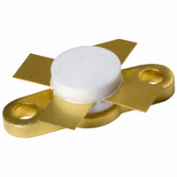
TRANSISTOR RF DMOS SOT123A
Manufacturer
NXP Semiconductors
Datasheet
1.BLF244112.pdf
(16 pages)
Specifications of BLF244,112
Package / Case
SOT-123A
Transistor Type
N-Channel
Frequency
175MHz
Gain
17dB
Voltage - Rated
65V
Current Rating
3A
Current - Test
25mA
Voltage - Test
28V
Power - Output
15W
Minimum Operating Temperature
- 65 C
Mounting Style
SMD/SMT
Resistance Drain-source Rds (on)
1.5 Ohm @ 10 V
Transistor Polarity
N-Channel
Configuration
Single Dual Source
Drain-source Breakdown Voltage
65 V
Gate-source Breakdown Voltage
+/- 20 V
Continuous Drain Current
3 A
Power Dissipation
38000 mW
Maximum Operating Temperature
+ 200 C
Application
VHF
Channel Type
N
Channel Mode
Enhancement
Drain Source Voltage (max)
65V
Output Power (max)
15W
Power Gain (typ)@vds
17@28V/15@12.5VdB
Frequency (max)
175MHz
Package Type
SOT-123A
Pin Count
4
Forward Transconductance (typ)
0.6(Min)S
Drain Source Resistance (max)
1500@10Vmohm
Input Capacitance (typ)@vds
60@28VpF
Output Capacitance (typ)@vds
40@28VpF
Reverse Capacitance (typ)
4.5@28VpF
Operating Temp Range
-65C to 200C
Drain Efficiency (typ)
65%
Mounting
Screw
Mode Of Operation
CW Class-B
Number Of Elements
1
Power Dissipation (max)
38000mW
Vswr (max)
50
Screening Level
Military
Lead Free Status / RoHS Status
Lead free / RoHS Compliant
Noise Figure
-
Lead Free Status / Rohs Status
Lead free / RoHS Compliant
Other names
568-2411
933817040112
BLF244
BLF244
933817040112
BLF244
BLF244


Philips Semiconductors
2003 Oct 13
handbook, halfpage
handbook, halfpage
VHF power MOS transistor
V
Fig.4
V
Fig.6
(mV/K)
R DS(on)
T.C.
DS
GS
( )
= 10 V; valid for T
= 10 V; I
2
0
2
4
6
8
1
2
1
0
Temperature coefficient of gate-source
voltage as a function of drain current, typical
values.
Drain-source on-state resistance as a
function of junction temperature, typical
values.
0
D
= 0.75 A.
j
40
= 25 to 125 C.
10
80
10
2
I D (mA)
120
T j ( C)
MGP152
MGP154
10
160
3
5
handbook, halfpage
handbook, halfpage
V
solid line: T
dotted line: T
Fig.5
V
Fig.7
DS
GS
(pF)
(A)
160
120
I D
C
= 10 V.
= 0; f = 1 MHz.
80
40
6
4
2
0
0
0
0
Drain current as a function of gate-source
voltage, typical values.
Input and output capacitance as functions
of drain-source voltage, typical values.
j
= 25 C.
j
= 125 C.
10
4
20
8
C os
C is
Product specification
12
30
V GS (V)
V DS (V)
BLF244
MGP153
MGP155
16
40
Related parts for BLF244,112
Image
Part Number
Description
Manufacturer
Datasheet
Request
R

Part Number:
Description:
Silicon N-channel enhancement mode vertical D-MOS transistor designed for large signal amplifier applications in the VHF frequency range
Manufacturer:
NXP Semiconductors
Datasheet:

Part Number:
Description:
NXP Semiconductors designed the LPC2420/2460 microcontroller around a 16-bit/32-bitARM7TDMI-S CPU core with real-time debug interfaces that include both JTAG andembedded trace
Manufacturer:
NXP Semiconductors
Datasheet:

Part Number:
Description:
NXP Semiconductors designed the LPC2458 microcontroller around a 16-bit/32-bitARM7TDMI-S CPU core with real-time debug interfaces that include both JTAG andembedded trace
Manufacturer:
NXP Semiconductors
Datasheet:
Part Number:
Description:
NXP Semiconductors designed the LPC2468 microcontroller around a 16-bit/32-bitARM7TDMI-S CPU core with real-time debug interfaces that include both JTAG andembedded trace
Manufacturer:
NXP Semiconductors
Datasheet:
Part Number:
Description:
NXP Semiconductors designed the LPC2470 microcontroller, powered by theARM7TDMI-S core, to be a highly integrated microcontroller for a wide range ofapplications that require advanced communications and high quality graphic displays
Manufacturer:
NXP Semiconductors
Datasheet:
Part Number:
Description:
NXP Semiconductors designed the LPC2478 microcontroller, powered by theARM7TDMI-S core, to be a highly integrated microcontroller for a wide range ofapplications that require advanced communications and high quality graphic displays
Manufacturer:
NXP Semiconductors
Datasheet:
Part Number:
Description:
The Philips Semiconductors XA (eXtended Architecture) family of 16-bit single-chip microcontrollers is powerful enough to easily handle the requirements of high performance embedded applications, yet inexpensive enough to compete in the market for hi
Manufacturer:
NXP Semiconductors
Datasheet:
Part Number:
Description:
The XA-S3 device is a member of Philips Semiconductors? XA(eXtended Architecture) family of high performance 16-bitsingle-chip microcontrollers
Manufacturer:
NXP Semiconductors
Datasheet:

Part Number:
Description:
The NXP BlueStreak LH75401/LH75411 family consists of two low-cost 16/32-bit System-on-Chip (SoC) devices
Manufacturer:
NXP Semiconductors
Datasheet:
Part Number:
Description:
The NXP LPC3130/3131 combine an 180 MHz ARM926EJ-S CPU core, high-speed USB2
Manufacturer:
NXP Semiconductors
Datasheet:
Part Number:
Description:
The NXP LPC3141 combine a 270 MHz ARM926EJ-S CPU core, High-speed USB 2
Manufacturer:
NXP Semiconductors
Part Number:
Description:
The NXP LPC3143 combine a 270 MHz ARM926EJ-S CPU core, High-speed USB 2
Manufacturer:
NXP Semiconductors

Part Number:
Description:
The NXP LPC3152 combines an 180 MHz ARM926EJ-S CPU core, High-speed USB 2
Manufacturer:
NXP Semiconductors
Part Number:
Description:
The NXP LPC3154 combines an 180 MHz ARM926EJ-S CPU core, High-speed USB 2
Manufacturer:
NXP Semiconductors