MW6S004NT1 Freescale Semiconductor, MW6S004NT1 Datasheet
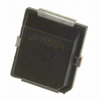
MOSFET RF N-CH 28V 4W PLD-1.5

MW6S004NT1

Manufacturer Part Number
MW6S004NT1
Description
MOSFET RF N-CH 28V 4W PLD-1.5
Manufacturer
Freescale Semiconductor
Datasheet

Specifications of MW6S004NT1

Transistor Type
N-Channel
Frequency
1.96GHz
Gain
18dB
Voltage - Rated
68V
Current Rating
10µA
Current - Test
50mA
Voltage - Test
28V
Power - Output
4W
Package / Case
PLD-1.5
Configuration
Single Dual Source
Drain-source Breakdown Voltage
68 V
Gate-source Breakdown Voltage
- 0.5 V or 12 V
Maximum Operating Temperature
+ 200 C
Minimum Operating Temperature
- 65 C
Mounting Style
SMD/SMT
Transistor Polarity
N-Channel
Drain Source Voltage Vds
68V
Rf Transistor Case
PLD-1.5
Termination Type
SMD
Output Power Pout
4W
Peak Reflow Compatible (260 C)
Yes
Rohs Compliant
Yes
Channel Type
N
Channel Mode
Enhancement
Drain Source Voltage (max)
68V
Power Gain (typ)@vds
19dB
Frequency (min)
1MHz
Frequency (max)
2GHz
Package Type
PLD-1.5
Pin Count
3
Input Capacitance (typ)@vds
23@28VpF
Output Capacitance (typ)@vds
25@28VpF
Reverse Capacitance (typ)
21@28VpF
Operating Temp Range
-65C to 150C
Drain Efficiency (typ)
33%
Mounting
Surface Mount
Mode Of Operation
2-Tone
Number Of Elements
1
Vswr (max)
5
Screening Level
Military
Filter Terminals
SMD
Gate-source Voltage
12V
Leaded Process Compatible
Yes
Operating Frequency Max
1.96GHz
Lead Free Status / RoHS Status
Lead free / RoHS Compliant
Noise Figure
-
Lead Free Status / Rohs Status
Lead free / RoHS Compliant
Other names
MW6S004NT1
MW6S004NT1TR

Available stocks

Company
Part Number
Manufacturer
Quantity
Price
Part Number:
MW6S004NT1
Manufacturer:
MINI
Quantity:
1 000
Part Number:
MW6S004NT1
Manufacturer:
Peregrine
Quantity:
6 700
Part Number:
MW6S004NT1
Manufacturer:
FREESCALE
Quantity:
20 000
© Freescale Semiconductor, Inc., 2007, 2009. All rights reserved.
RF Device Data
Freescale Semiconductor
Technical Data
RF Power Field Effect Transistor
N - Channel Enhancement - Mode Lateral MOSFET
up to 2000 MHz. Suitable for analog and digital modulation and multicarrier
amplifier applications.
• Typical Two - Tone Performance @ 1960 MHz, 28 Volts, I
• Typical Two - Tone Performance @ 900 MHz, 28 Volts, I
• Capable of Handling 5:1 VSWR, @ 28 Vdc, 1960 MHz, 4 Watts CW Output
Features
• Characterized with Series Equivalent Large - Signal Impedance Parameters
• On - Chip RF Feedback for Broadband Stability
• Integrated ESD Protection
• RoHS Compliant
• In Tape and Reel. T1 Suffix = 1000 Units per 12 mm, 7 inch Reel.
Table 1. Maximum Ratings
Table 2. Thermal Characteristics
Table 3. ESD Protection Characteristics
Drain - Source Voltage
Gate - Source Voltage
Storage Temperature Range
Operating Junction Temperature
Thermal Resistance, Junction to Case
Human Body Model (per JESD22 - A114)
Machine Model (per EIA/JESD22 - A115)
Charge Device Model (per JESD22 - C101)
Designed for Class A or Class AB base station applications with frequencies
1. MTTF calculator available at http://www.freescale.com/rf. Select Software & Tools/Development Tools/Calculators to access
2. Refer to AN1955, Thermal Measurement Methodology of RF Power Amplifiers. Go to http://www.freescale.com/rf.
P
P
Power
Case Temperature 76°C, 4 W PEP, Two - Tone
Case Temperature 79°C, 4 W CW
out
out
Power Gain — 18 dB
Drain Efficiency — 33%
IMD — - 34 dBc
Power Gain — 19 dB
Drain Efficiency — 33%
IMD — - 39 dBc
MTTF calculators by product.
Select Documentation/Application Notes - AN1955.
= 4 Watts PEP
= 4 Watts PEP
Test Methodology
Characteristic
Rating
DQ
DQ
= 50 mA,
= 50 mA,
Symbol
Symbol
V
R
V
T
DSS
T
θJC
GS
stg
J
Document Number: MW6S004N
MW6S004NT1
LATERAL N - CHANNEL
1 - 2000 MHz, 4 W, 28 V
RF POWER MOSFET
CASE 466 - 03, STYLE 1
1C (Minimum)
IV (Minimum)
A (Minimum)
- 65 to +150
Value
- 0.5, +68
- 0.5, +12
Value
Class
150
8.8
8.5
PLASTIC
PLD 1.5
(1,2)
Rev. 4, 6/2009
MW6S004NT1
°C/W
Unit
Unit
Vdc
Vdc
°C
°C
1

Related parts for MW6S004NT1

MW6S004NT1 Summary of contents

Page 1

... LATERAL N - CHANNEL RF POWER MOSFET = 50 mA, DQ CASE 466 - 03, STYLE 1 Symbol V DSS stg T J Symbol R θJC 1C (Minimum) Rev. 4, 6/2009 PLD 1.5 PLASTIC Value Unit - 0.5, +68 Vdc - 0.5, +12 Vdc - 65 to +150 °C 150 °C (1,2) Value Unit °C/W 8.8 8.5 Class A (Minimum) IV (Minimum) MW6S004NT1 1 ...

Page 2

... MHz, Two - Tone Test, 100 kHz Tone Spacing Power Gain Drain Efficiency Intermodulation Distortion Input Return Loss Parameter measured on Freescale Test Fixture, due to resistive divider network on the board GS(Q) Refer to Test Circuit Schematic. MW6S004NT1 2 Rating 3 = 25°C unless otherwise noted) A Symbol I DSS I DSS I GSS V GS(th) ...

Page 3

... Microstrip Z3 0.580″ x 0.420″ Microstrip Z4 0.580″ x 0.100″ Microstrip Z5 0.025″ x 0.680″ Microstrip Z6 0.210″ x 0.100″ Microstrip Table 6. MW6S004NT1 Test Circuit Component Designations and Values Part C1 100 nF Chip Capacitor C2, C3, C6, C7 9.1 pF Chip Capacitors C4 μ Chip Capacitors C8 10 μ ...

Page 4

... MW6S004N Rev 3 Figure 2. MW6S004NT1 Test Circuit Component Layout MW6S004NT1 Device Data Freescale Semiconductor ...

Page 5

... Vdc 5th Order 7th Order 0 OUTPUT POWER (WATTS) PEP out versus Output Power P6dB = 38.73 dBm (7.465 W) P3dB = 38.22 dBm (6.637 Vdc Pulsed CW, 8 μsec(on), 1 msec(off 1960 MHz INPUT POWER (dBm) in Input Power MW6S004NT1 10 Ideal Actual 26 5 ...

Page 6

... Figure 8. Single - Carrier CDMA ACPR, Power Gain 0.01 19 18.5 18 17.5 17 16 OUTPUT POWER (WATTS) CW out Figure 10. Power Gain versus Output Power MW6S004NT1 6 TYPICAL CHARACTERISTICS = 28 Vdc ACPR η OUTPUT POWER (WATTS) AVG. out and Drain Efficiency versus Output Power T = −30_C 25_C 85_C Vdc η ...

Page 7

... T , JUNCTION TEMPERATURE (°C) J This above graph displays calculated MTTF in hours when the device = 4 W PEP, and η is operated Vdc out MTTF calculator available at http://www.freescale.com/rf. Select Software & Tools/Development Tools/Calculators to access MTTF calculators by product. 230 250 = 33%. D MW6S004NT1 7 ...

Page 8

... Z o Figure 13. Series Equivalent Source and Load Impedance MW6S004NT1 1990 MHz Z load = 10 Ω 1930 MHz f = 1990 MHz Z source f = 1930 MHz Vdc mA PEP DD DQ out source load MHz W W 1930 1.96 - j5.34 8.78 + j6.96 1960 1.89 - j5.10 8.93 + j7.46 1990 1.82 - j4.85 9 ...

Page 9

... MW6S004NT1 9 ...

Page 10

... MW6S004NT1 ohm system) (continued ∠ φ 1.211 - 25.120 0.006 1.187 - 26.920 0.006 1.166 - 28.650 0.006 1 ...

Page 11

... N 0.230 0.240 5.84 6.10 P 0.000 0.008 0.00 0.20 Q 0.055 0.063 1.40 1.60 R 0.200 0.210 5.08 5.33 S 0.006 0.012 0.15 0.31 U 0.006 0.012 0.15 0.31 ZONE V 0.000 0.021 0.00 0.53 ZONE W 0.000 0.010 0.00 0.25 ZONE X 0.000 0.010 0.00 0.25 MW6S004NT1 11 ...

Page 12

... Modified data sheet to reflect MSL rating change from result of the standardization of packing process as described in Product and Process Change Notification number, PCN13516 • Added Electromigration MTTF Calculator and RF High Power Model availability to Product Documentation, Tools and Software MW6S004NT1 12 REVISION HISTORY Description ...

Page 13

... Freescale Semiconductor was negligent regarding the design or manufacture of the part. Freescalet and the Freescale logo are trademarks of Freescale Semiconductor, Inc. All other product or service names are the property of their respective owners. © Freescale Semiconductor, Inc. 2007, 2009. All rights reserved. MW6S004NT1 13 ...

Related keywords