MW6S004NT1 Freescale Semiconductor, MW6S004NT1 Datasheet - Page 2
MW6S004NT1
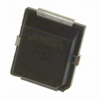
Manufacturer Part Number
MW6S004NT1
Description
MOSFET RF N-CH 28V 4W PLD-1.5
Manufacturer
Freescale Semiconductor
Datasheet
1.MW6S004NT1.pdf
(13 pages)
Specifications of MW6S004NT1
Transistor Type
N-Channel
Frequency
1.96GHz
Gain
18dB
Voltage - Rated
68V
Current Rating
10µA
Current - Test
50mA
Voltage - Test
28V
Power - Output
4W
Package / Case
PLD-1.5
Configuration
Single Dual Source
Drain-source Breakdown Voltage
68 V
Gate-source Breakdown Voltage
- 0.5 V or 12 V
Maximum Operating Temperature
+ 200 C
Minimum Operating Temperature
- 65 C
Mounting Style
SMD/SMT
Transistor Polarity
N-Channel
Drain Source Voltage Vds
68V
Rf Transistor Case
PLD-1.5
Termination Type
SMD
Output Power Pout
4W
Peak Reflow Compatible (260 C)
Yes
Rohs Compliant
Yes
Channel Type
N
Channel Mode
Enhancement
Drain Source Voltage (max)
68V
Power Gain (typ)@vds
19dB
Frequency (min)
1MHz
Frequency (max)
2GHz
Package Type
PLD-1.5
Pin Count
3
Input Capacitance (typ)@vds
23@28VpF
Output Capacitance (typ)@vds
25@28VpF
Reverse Capacitance (typ)
21@28VpF
Operating Temp Range
-65C to 150C
Drain Efficiency (typ)
33%
Mounting
Surface Mount
Mode Of Operation
2-Tone
Number Of Elements
1
Vswr (max)
5
Screening Level
Military
Filter Terminals
SMD
Gate-source Voltage
12V
Leaded Process Compatible
Yes
Operating Frequency Max
1.96GHz
Lead Free Status / RoHS Status
Lead free / RoHS Compliant
Noise Figure
-
Lead Free Status / Rohs Status
Lead free / RoHS Compliant
Other names
MW6S004NT1
MW6S004NT1TR
MW6S004NT1TR
Available stocks
Company
Part Number
Manufacturer
Quantity
Price
Company:

Part Number:
MW6S004NT1
Manufacturer:
MINI
Quantity:
1 000
Company:
Part Number:
MW6S004NT1
Manufacturer:
Peregrine
Quantity:
6 700
Part Number:
MW6S004NT1
Manufacturer:
FREESCALE
Quantity:
20 000


MW6S004NT1
2
Table 4. Moisture Sensitivity Level
Table 5. Electrical Characteristics
Off Characteristics
On Characteristics
Dynamic Characteristics
Functional Tests (In Freescale Test Fixture, 50 ohm system) V
f2 = 1960.1 MHz, Two - Tone Test
Typical Performance (In Freescale 900 MHz Demo Board, 50 ohm system) V
f = 900 MHz, Two - Tone Test, 100 kHz Tone Spacing
Per JESD 22 - A113, IPC/JEDEC J - STD - 020
Zero Gate Voltage Drain Leakage Current
Zero Gate Voltage Drain Leakage Current
Gate - Source Leakage Current
Gate Threshold Voltage
Gate Quiescent Voltage
Fixture Gate Quiescent Voltage
Drain - Source On - Voltage
Reverse Transfer Capacitance
Output Capacitance
Input Capacitance
Power Gain
Drain Efficiency
Intermodulation Distortion
Input Return Loss
Power Gain
Drain Efficiency
Intermodulation Distortion
Input Return Loss
1. V
(V
(V
(V
(V
(V
(V
(V
(V
(V
(V
Refer to Test Circuit Schematic.
DS
DS
GS
DS
DS
DD
GS
DS
DS
DS
GG
= 68 Vdc, V
= 28 Vdc, V
= 10 Vdc, I
= 28 Vdc, I
= 28 Vdc ± 30 mV(rms)ac @ 1 MHz, V
= 28 Vdc ± 30 mV(rms)ac @ 1 MHz, V
= 28 Vdc, V
= 5 Vdc, V
= 28 Vdc, I
= 10 Vdc, I
=
11
/
10
x V
DS
D
D
D
D
GS(Q)
GS
GS
GS
= 50 mAdc)
= 50 mAdc)
= 50 mAdc, Measured in Functional Test)
= 50 mAdc)
= 0 Vdc)
= 0 Vdc)
= 0 Vdc)
= 0 Vdc ± 30 mV(rms)ac @ 1 MHz)
. Parameter measured on Freescale Test Fixture, due to resistive divider network on the board.
Test Methodology
Characteristic
(1)
(T
A
= 25°C unless otherwise noted)
GS
GS
= 0 Vdc)
= 0 Vdc)
DD
= 28 Vdc, I
Symbol
DQ
V
Rating
V
V
DD
V
I
I
I
C
DS(on)
C
IMD
IMD
GS(th)
GS(Q)
GG(Q)
C
G
G
IRL
IRL
DSS
DSS
GSS
η
η
= 50 mA, P
3
oss
rss
iss
= 28 Vdc, I
ps
D
ps
D
out
DQ
16.5
Min
Package Peak Temperature
1.2
2.2
—
—
—
—
—
—
—
—
28
—
—
—
—
—
—
= 4 W PEP, f1 = 1960 MHz,
= 50 mA, P
0.27
260
Typ
- 34
- 12
- 39
- 12
2.7
21
25
30
18
33
19
33
—
—
—
out
2
3
= 4 W PEP,
Freescale Semiconductor
Max
0.37
500
- 28
- 10
2.7
4.2
10
10
20
—
—
—
—
—
—
—
—
—
RF Device Data
μAdc
μAdc
nAdc
Unit
Unit
Vdc
Vdc
Vdc
Vdc
dBc
dBc
dB
dB
dB
dB
°C
pF
pF
pF
%
%
Related parts for MW6S004NT1
Image
Part Number
Description
Manufacturer
Datasheet
Request
R


Part Number:
Description:
RELAY HI FREQ 6GHZ DPDT
Manufacturer:
TE Connectivity
Datasheet:

Part Number:
Description:
Manufacturer:
Freescale Semiconductor, Inc
Datasheet:
Part Number:
Description:
Manufacturer:
Freescale Semiconductor, Inc
Datasheet:
Part Number:
Description:
Manufacturer:
Freescale Semiconductor, Inc
Datasheet:
Part Number:
Description:
Manufacturer:
Freescale Semiconductor, Inc
Datasheet:
Part Number:
Description:
Manufacturer:
Freescale Semiconductor, Inc
Datasheet:
Part Number:
Description:
Manufacturer:
Freescale Semiconductor, Inc
Datasheet:
Part Number:
Description:
Manufacturer:
Freescale Semiconductor, Inc
Datasheet:
Part Number:
Description:
Manufacturer:
Freescale Semiconductor, Inc
Datasheet:
Part Number:
Description:
Manufacturer:
Freescale Semiconductor, Inc
Datasheet:
Part Number:
Description:
Manufacturer:
Freescale Semiconductor, Inc
Datasheet:
Part Number:
Description:
Manufacturer:
Freescale Semiconductor, Inc
Datasheet:
Part Number:
Description:
Manufacturer:
Freescale Semiconductor, Inc
Datasheet:
Part Number:
Description:
Manufacturer:
Freescale Semiconductor, Inc
Datasheet: