BLF6G10-135RN,112 NXP Semiconductors, BLF6G10-135RN,112 Datasheet
BLF6G10-135RN,112
Specifications of BLF6G10-135RN,112


Related parts for BLF6G10-135RN,112


BLF6G10-135RN,112 Summary of contents
Page 1
... BLF6G10-135RN; BLF6G10LS-135RN Power LDMOS transistor Rev. 02 — 21 January 2010 1. Product profile 1.1 General description 135 W LDMOS power transistor for base station applications at frequencies from 700 MHz to 1000 MHz. Table 1. Typical RF performance at T Mode of operation 2-carrier W-CDMA [1] Test signal: 3GPP; test model 1; 64 DPCH; PAR = 7 0.01 % probability on CCDF per carrier; carrier spacing 5 MHz ...
Page 2
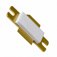
... NXP Semiconductors 1.3 Applications RF power amplifiers for GSM, GSM EDGE, W-CDMA and CDMA base stations and multi carrier applications in the 700 MHz to 1000 MHz frequency range 2. Pinning information Table 2. Pin BLF6G10-135RN (SOT502A BLF6G10LS-135RN (SOT502B [1] Connected to flange. 3. Ordering information Table 3. Type number ...
Page 3
... Symbol P L(AV η D ACPR 7.1 Ruggedness in class-AB operation The BLF6G10-135RN and BLF6G10LS-135RN are capable of withstanding a load mismatch corresponding to VSWR = through all phases under the following conditions: V BLF6G10-135RN_10LS-135RN_2 Product data sheet Thermal characteristics Conditions thermal resistance from T case junction to case Characteristics C unless otherwise specified ...
Page 4
... One-tone CW power gain and drain efficiency as function of load power; typical values 001aah865 60 η IMD D (%) (dBc 100 P (W) L(PEP) = 881 MHz (±100 kHz). 1 Fig 3. Rev. 02 — 21 January 2010 BLF6G10(LS)-135RN Power LDMOS transistor 001aah864 75 η D (%) 120 160 P (W) L −20 −30 −40 −50 − ...
Page 5
... P (W) L(AV) = 881 MHz 886 MHz Fig C12 Rev. 02 — 21 January 2010 BLF6G10(LS)-135RN Power LDMOS transistor −20 ACPR (dBc) −30 −40 − 950 mA 881 MHz carrier spacing 5 MHz. 2-carrier W-CDMA adjacent power channel ratio as a function of average load power; typical values ...
Page 6
... 800 -1000 MHz V1.0 Value 100 nF 4.7 μ 3.0 pF 220 μ 9.1 Ω; 0.1 W Rev. 02 — 21 January 2010 BLF6G10(LS)-135RN Power LDMOS transistor C18 C10 C11 C6 C7 C19 C14 C15 C12 C13 OUT 800 -1000 MHz V1.0 = 3.5 and thickness = 0.76 mm. ...
Page 7
... REFERENCES JEDEC JEITA Rev. 02 — 21 January 2010 BLF6G10(LS)-135RN Power LDMOS transistor 3.38 1.70 34.16 9.91 27.94 0.25 3 ...
Page 8
... REFERENCES JEDEC JEITA Rev. 02 — 21 January 2010 BLF6G10(LS)-135RN Power LDMOS transistor 1.70 20.70 9.91 0.25 1.45 20.45 9.65 0.067 0.815 0.390 0.010 0.057 ...
Page 9
... LDMOS LDMOST PAR PDPCH RF SMD VSWR W-CDMA 11. Revision history Table 10. Revision history Document ID BLF6G10-135RN_10LS-135RN_2 20100121 Modifications BLF6G10-135RN_10LS-135RN_1 20090210 BLF6G10-135RN_10LS-135RN_2 Product data sheet Abbreviations Description Third Generation Partnership Project Complementary Cumulative Distribution Function Code Division Multiple Access Continuous Wave Dedicated Physical CHannel ...
Page 10
... Trademarks Notice: All referenced brands, product names, service names and trademarks are the property of their respective owners. http://www.nxp.com salesaddresses@nxp.com Rev. 02 — 21 January 2010 BLF6G10(LS)-135RN Power LDMOS transistor © NXP B.V. 2010. All rights reserved ...
Page 11
... Please be aware that important notices concerning this document and the product(s) described herein, have been included in section ‘Legal information’. © NXP B.V. 2010. For more information, please visit: http://www.nxp.com For sales office addresses, please send an email to: salesaddresses@nxp.com Document identifier: BLF6G10-135RN_10LS-135RN_2 All rights reserved. Date of release: 21 January 2010 ...