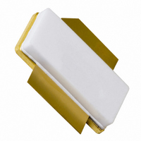
BLF6G10LS-200R,118 NXP Semiconductors, BLF6G10LS-200R,118 Datasheet - Page 3

BLF6G10LS-200R,118
Manufacturer Part Number
BLF6G10LS-200R,118
Description
IC BASESTATION FINAL SOT502B
Manufacturer
NXP Semiconductors
Datasheet
1.BLF6G10LS-200R118.pdf
(10 pages)
Specifications of BLF6G10LS-200R,118
Package / Case
SOT502B
Transistor Type
LDMOS
Frequency
871.5MHz
Gain
20dB
Voltage - Rated
65V
Current Rating
49A
Current - Test
1.4A
Voltage - Test
28V
Power - Output
40W
Configuration
Single
Transistor Polarity
N-Channel
Resistance Drain-source Rds (on)
0.06 Ohms
Drain-source Breakdown Voltage
65 V
Gate-source Breakdown Voltage
- 0.5 V to + 13 V
Continuous Drain Current
49 A
Maximum Operating Temperature
+ 225 C
Mounting Style
SMD/SMT
Minimum Operating Temperature
- 65 C
Lead Free Status / RoHS Status
Lead free / RoHS Compliant
Noise Figure
-
Lead Free Status / RoHS Status
Lead free / RoHS Compliant, Lead free / RoHS Compliant
Other names
934061248118
BLF6G10LS-200R /T3
BLF6G10LS-200R /T3
BLF6G10LS-200R /T3
BLF6G10LS-200R /T3
NXP Semiconductors
6. Characteristics
7. Application information
BLF6G10LS-200R_1
Preliminary data sheet
7.1 Ruggedness in class-AB operation
Table 6.
T
Table 7.
Mode of operation: 2-carrier W-CDMA; PAR 7.5 dB at 0.01 % probability on CCDF; 3GPP test
model 1; 1-64 PDPCH; f
RF performance at V
class-AB production test circuit.
The BLF6G10LS-200R is an enhanced rugged device and is capable of withstanding a
load mismatch corresponding to VSWR = 10 : 1 through all phases under the following
conditions: V
Symbol Parameter
V
V
V
I
I
I
g
R
C
Symbol
P
G
IRL
ACPR
DSS
DSX
GSS
j
fs
D
(BR)DSS
GS(th)
GSq
L(AV)
DS(on)
rs
p
= 25 C unless otherwise specified.
drain-source breakdown
voltage
gate-source threshold voltage
gate-source quiescent voltage V
drain leakage current
drain cut-off current
gate leakage current
forward transconductance
drain-source on-state
resistance
feedback capacitance
Parameter
average output power
power gain
input return loss
drain efficiency
adjacent channel power ratio
Characteristics
Application information
DS
= 28 V; I
DS
= 28 V; I
1
Rev. 01 — 21 January 2008
= 871.5 MHz; f
Dq
= 1400 mA; P
Dq
= 1400 mA; T
2
= 876.5 MHz; f
Conditions
V
V
I
V
V
V
V
V
V
I
V
f = 1 MHz
D
D
GS
DS
DS
GS
GS
DS
GS
DS
GS
GS
L
= 1620 mA
= 9.45 A
= 200 W; f = 894 MHz.
= 10 V; I
= 28 V;
= 10 V
= 10 V; I
= 0 V; I
= 0 V; V
= V
= 11 V; V
= V
= 0 V; V
case
GS(th)
GS(th)
Conditions
P
P
P
P
= 25 C; unless otherwise specified; in a
L(AV)
L(AV)
L(AV)
L(AV)
D
DS
DS
D
D
= 0.9 mA
+ 3.75 V;
+ 3.75 V;
DS
3
BLF6G10LS-200R
= 270 mA
= 9.45 A
= 40 W
= 40 W
= 40 W
= 40 W
= 886.5 MHz; f
= 28 V
= 28 V;
= 0 V
Power LDMOS transistor
Min
65
1.4
1.7
-
40
-
11
0.012 0.07
-
Min
-
19
-
25
-
4
= 891.5 MHz;
Typ
40
20
27.5
Typ
-
2.0
2.2
-
48
-
18
3
© NXP B.V. 2008. All rights reserved.
6.7
40.5
Max
-
21
-
Max
-
2.4
2.7
4.2
-
420
26
0.093
-
5.0
38.0 dBc
3 of 10
Unit
W
dB
dB
%
Unit
V
V
V
A
nA
S
pF
A


