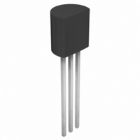
MPSH11 Fairchild Semiconductor, MPSH11 Datasheet

MPSH11
Specifications of MPSH11
Available stocks
Related parts for MPSH11
MPSH11 Summary of contents
Page 1
... Device mounted on FR-4 PCB 1.6" X 1.6" X 0.06." 2002 Fairchild Semiconductor Corporation MMBTH11 C TO-92 SOT-23 Mark 25°C unless otherwise noted Parameter TA = 25°C unless otherwise noted MPSH11 350 2.8 125 357 E B Value Units 3 -55 to +150 C Max Units *MMBTH11 225 mW 1.8 mW/ C C/W 556 C/W MPSH11/MMBTH11, Rev. B ...
Page 2
... MHz 1.0 MHz 1.0 MHz 4.0 mA 31.8 MHz Collector-Emitter Saturation Voltage vs Collector Current 0 0.15 0.1 0. °C 10 100 0 NPN RF Transistor (continued) Min Max Units 3.0 V 100 nA 100 nA 60 0.5 V 0.95 V 650 MHz 0.7 pF 0.6 0.9 pF 9.0 pS 125 ° COLLECTOR CURRENT (mA) MPSH11/MMBTH11, Rev ...
Page 3
... Collector Current - 40 °C 25 125 ° 5. 100 - COLLECTOR CURRENT (mA) TO- 100 125 150 TEMPERATURE ( C) ° T 1000 MHz 900 MHz 800 MHz 700 MHz 600 MHz 500 MHz 300 MHz 400 MHz 200 MHz 100 MHz 1 10 100 MPSH11/MMBTH11, Rev. B ...
Page 4
... I - COLLECTOR CURRENT (mA) C Input Admittance 10V 200 MHz COLLECTOR CURRENT (mA) C Input Admittance 15V 7 100 Forward Transfer Admittance vs Collector Current 120 V = 10V 200 MHz 100 COLLECTOR CURRENT (mA) NPN RF Transistor (continued) Collector Current Frequency 200 500 1000 f - FREQUENCY (MHz MPSH11/MMBTH11, Rev ...
Page 5
... Reverse Transfer Admittance vs Collector Current 0 10V 200 MHz 0.5 0.4 0.3 0.2 0 COLLECTOR CURRENT (mA) C Reverse Transfer Admittance vs Frequency 1 15V 7 0.8 0.6 0.4 0 100 f - FREQUENCY (MHz) NPN RF Transistor (continued 200 500 1000 f - FREQUENCY (MHz 200 500 1000 MPSH11/MMBTH11, Rev. B ...
Page 6
... CE 0 MHz 0 COLLECTOR CURRENT (mA) C Output Admittance 10000 V = 15V MHz C 1000 100 10 50 100 20 24 Conversion Gain vs Collector Current COLLECTOR CURRENT (mA) C NPN RF Transistor (continued Frequency 200 500 1000 f - FREQUENCY (MHz MHz 200 MHz 245 MHz 15V CE FIG MPSH11/MMBTH11, Rev ...
Page 7
... Input L1 1000 pF 2 FIGURE 1: Unneutralized 200 MHz PG and NF Test Circuit 270 1000 pF 1000 0.8-10 pF 1000 pF 390 L1 - Ohmite Z-235 RFC turns No. 14 wire, 1 inch L x 1/4 inch ID tapped 1 1/2 turns from cold side BB NPN RF Transistor (continued) 200 mHz Output into 50 MPSH11/MMBTH11, Rev. B ...
Page 8
... No. 22 wire 8 turns Pri. 2 turns Sec mHz Output into Ohmite RFC Z235 T1 - Primary 5 turns No. 34 wire 1/4 inch diameter. Secondary runs No. 34 wire close wound over a Q100 core (10.7 mHz). When terminated on secondary side with 50 primary measures 1.5 K, -25 pF. MPSH11/MMBTH11, Rev ...


