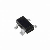
BFG520,215 NXP Semiconductors, BFG520,215 Datasheet - Page 6

BFG520,215
Manufacturer Part Number
BFG520,215
Description
TRANS NPN 15V 9GHZ SOT143B
Manufacturer
NXP Semiconductors
Datasheet
1.BFG520XR235.pdf
(14 pages)
Specifications of BFG520,215
Package / Case
SOT-143, SOT-143B, TO-253AA
Mounting Type
Surface Mount
Power - Max
300mW
Current - Collector (ic) (max)
70mA
Voltage - Collector Emitter Breakdown (max)
15V
Transistor Type
NPN
Frequency - Transition
9GHz
Dc Current Gain (hfe) (min) @ Ic, Vce
60 @ 20mA, 6V
Noise Figure (db Typ @ F)
1.6dB ~ 2.1dB @ 900MHz
Dc Collector/base Gain Hfe Min
120
Minimum Operating Temperature
- 65 C
Mounting Style
SMD/SMT
Configuration
Single
Transistor Polarity
NPN
Maximum Operating Frequency
9 GHz
Collector- Emitter Voltage Vceo Max
15 V
Emitter- Base Voltage Vebo
2.5 V
Continuous Collector Current
70 mA
Power Dissipation
300 mW
Number Of Elements
1
Collector-emitter Voltage
15V
Collector-base Voltage
20V
Emitter-base Voltage
2.5V
Collector Current (dc) (max)
70mA
Dc Current Gain (min)
60
Frequency (max)
9GHz
Operating Temp Range
-65C to 175C
Operating Temperature Classification
Military
Mounting
Surface Mount
Pin Count
3 +Tab
Package Type
SOT-143R
Lead Free Status / RoHS Status
Lead free / RoHS Compliant
Gain
-
Lead Free Status / Rohs Status
Compliant
Other names
934018800215::BFG520 T/R::BFG520 T/R
NXP Semiconductors
In Figs 7 to 10, G
MSG = maximum stable gain; G
gain.
handbook, halfpage
handbook, halfpage
NPN 9 GHz wideband transistor
V
I
C
CE
= 5 mA; V
gain
(dB)
gain
(dB)
= 6 V; f = 900 MHz; T
Fig.7 Gain as a function of collector current.
25
20
15
10
50
40
30
20
10
5
0
0
10
0
Fig.9 Gain as a function of frequency.
CE
G UM
MSG
MSG
= 6 V; T
UM
= maximum unilateral power gain;
amb
10
10
amb
2
= 25 C.
= 25 C.
max
10
20
= maximum available
3
I C (mA)
f (MHz)
G max
G max
G UM
MRA674
MRA676
Rev. 04 - 23 November 2007
10
30
4
handbook, halfpage
handbook, halfpage
V
I
C
CE
BFG520; BFG520/X; BFG520/XR
= 20 mA; V
gain
(dB)
gain
(dB)
Fig.8 Gain as a function of collector current.
= 6 V; f = 2 GHz; T
25
20
15
10
50
40
30
20
10
5
0
0
10
Fig.10 Gain as a function of frequency.
0
MSG
CE
= 6 V; T
amb
10
10
amb
2
G UM
MSG
= 25 C.
= 25 C.
G max
G UM
10
20
3
Product specification
I C (mA)
f (MHz)
G max
MRA675
MRA677
6 of 14
10
30
4


