MAT02FHZ Analog Devices Inc, MAT02FHZ Datasheet - Page 7
MAT02FHZ
Manufacturer Part Number
MAT02FHZ
Description
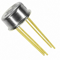
IC TRANS DUAL MATCHED NPN TO-78
Manufacturer
Analog Devices Inc
Datasheet
1.MAT02EH.pdf
(12 pages)
Specifications of MAT02FHZ
Transistor Type
2 NPN (Dual)
Current - Collector (ic) (max)
20mA
Voltage - Collector Emitter Breakdown (max)
40V
Vce Saturation (max) @ Ib, Ic
200mV @ 100µA, 1mA
Current - Collector Cutoff (max)
4nA
Power - Max
1.8W
Frequency - Transition
200MHz
Mounting Type
Through Hole
Package / Case
TO-78-6 Metal Can
Lead Free Status / RoHS Status
Lead free / RoHS Compliant
Dc Current Gain (hfe) (min) @ Ic, Vce
-


APPLICATIONS: NONLINEAR FUNCTIONS
MULTIPLIER/DIVIDER CIRCUIT
The excellent log conformity of the MAT02 over a very wide
range of collector current makes it ideal for use in log-antilog
circuits. Such nonlinear functions as multiplying, dividing,
squaring and square-rooting are accurately and easily imple-
mented with a log antilog circuit using two MAT02 pairs (see
Figure 3). The transistor circuit accepts three input currents (I
I
I
circuit, but negative input voltages can be easily accommodated
by various offsetting techniques. Protective diodes across each
base-to-emitter junction would normally be needed, but these
diodes are built into the MAT02. External protection diodes
are, therefore, not needed.
For the circuit shown in Figure 3, the operational amplifiers
make I
output voltage for this one-quadrant, log-antilog multiplier/
divider is ideally:
If all the resistors (R
Resistor values of 50 kΩ to 100 kΩ are recommended assuming
an input range of 0.1 V to +10 V.
ERROR ANALYSIS
The base-to-emitter voltage of the MAT02 in its forward active
operation is:
The first term comes from the idealized intrinsic transistor
equation previously discussed (see equation (1)).
Extrinsic resistive terms and the early effect cause departure
from the ideal logarithmic relationship. For small V
REV. E
2
O
and I
= I
1
I
1
2
3
= V
) and provides an output current I
/I
3
. All four currents must be positive in the log antilog
V
X
O
/R
V
=
BE
1
, I
R
R
=
2
3
1
R
R
= V
O
kT
V
O
2
, R
q
O
V
Y
In
= V
1
V
/R
X
, R
V
Z
I
I
2
C
S
X
Y
, I
2
, R
V
+ r
3
(V
Y
= V
/V
3
) are made equal, then
BE
X
Z
, V
I
Z
C
/R
, V
Y
, V
3
, and I
CB
Z
O
~ 0
> 0)
Figure 3. One-Quadrant Multiplier/Divider
according to
O
= V
CB
O
/R
, all of
O
. The
(4)
(5)
1
,
–7–
these effects can be lumped together as a total effective bulk
resistance r
logarithmic relationship. The r
than 0.5 Ω and ∆r
Returning to the multiplier/divider circuit of Figure 1 and using
Equation (4):
If the transistor pairs are held to the same temperature, then:
If all the terms on the right-hand side were zero, then In
(I
the desired result:
Note that this relationship is temperature independent. The
right-hand side of Equation (6) is near zero and the output
current I
define ø as the right-hand side terms of Equation (6):
For the MAT02, In (I
ø, ε
The In (I
± 0.6% from each pair when using the MAT02, and this gain
error is easily trimmed out by varying R
1
V
I
Ø
BE1A
2
kT
/I
~ 1 + ø and therefore:
q
3
ø = In
I
+ V
O
In
O
SA
) would equal zero, which would lead directly to
will be approximately I
BE
/I
I
I I
BE2A
I I
O
SB
. The r
3
1 2
I
I
=
) terms in ø cause a fixed gain error of less than
O
S A S A
S B S B
1
1
I
– V
=
BE
I
1
I
I
I
O
I
3
kT
2
2
2
BE
between the two sides is negligible.
q
I
~
BE2B
I
, where I
3
1
SA
I
I
I
C
+
I
O
2
In
1
I
/I
I
3
term causes departure from the desired
kT
– V
SB
2
= 1 + ø
q
I
I
) and I
S A S A
S B S B
(1 – ø)
1
1
BE1B
(I
1
BE
I
I
, I
1
+ I
2
2
2
term for the MAT02 is less
1
+ (I
, I
C
I
r
+ (I
2
2
3
BE
/I
, I
– I
1
3
O
. To estimate error,
are very small. For small
+ I
1
O
> 0
O
+ I
– I
2
. The I
– I
2
3
) r
– I
O
BE
– I
O
MAT02
OUT
– I
3
) r
3
) r
terms are
BE
BE
= 0
(6)
(7)
(8)
(9)
Related parts for MAT02FHZ
Image
Part Number
Description
Manufacturer
Datasheet
Request
R

Part Number:
Description:
±1.7g Dual-Axis IMEMS Accelerometer Evaluation Board
Manufacturer:
Analog Devices Inc
Datasheet:

Part Number:
Description:
Inertial Sensor Evaluation System
Manufacturer:
Analog Devices Inc
Datasheet:
Part Number:
Description:
Manufacturer:
Analog Devices Inc
Datasheet:
Part Number:
Description:
Manufacturer:
Analog Devices Inc
Datasheet:
Part Number:
Description:
Manufacturer:
Analog Devices Inc
Datasheet:
Part Number:
Description:
Manufacturer:
Analog Devices Inc
Datasheet:
Part Number:
Description:
Manufacturer:
Analog Devices Inc
Datasheet:
Part Number:
Description:
Manufacturer:
Analog Devices Inc
Datasheet:
Part Number:
Description:
Manufacturer:
Analog Devices Inc
Datasheet:
Part Number:
Description:
Manufacturer:
Analog Devices Inc
Datasheet:
Part Number:
Description:
Manufacturer:
Analog Devices Inc
Datasheet:
Part Number:
Description:
Manufacturer:
Analog Devices Inc
Datasheet:
Part Number:
Description:
Manufacturer:
Analog Devices Inc
Datasheet: