MAT02FHZ Analog Devices Inc, MAT02FHZ Datasheet - Page 9
MAT02FHZ
Manufacturer Part Number
MAT02FHZ
Description
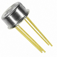
IC TRANS DUAL MATCHED NPN TO-78
Manufacturer
Analog Devices Inc
Datasheet
1.MAT02EH.pdf
(12 pages)
Specifications of MAT02FHZ
Transistor Type
2 NPN (Dual)
Current - Collector (ic) (max)
20mA
Voltage - Collector Emitter Breakdown (max)
40V
Vce Saturation (max) @ Ib, Ic
200mV @ 100µA, 1mA
Current - Collector Cutoff (max)
4nA
Power - Max
1.8W
Frequency - Transition
200MHz
Mounting Type
Through Hole
Package / Case
TO-78-6 Metal Can
Lead Free Status / RoHS Status
Lead free / RoHS Compliant
Dc Current Gain (hfe) (min) @ Ic, Vce
-


Collector current range is the key design decision. The inher-
ently low r
collector current. For input scaling of ± 10 V full-scale and using
a 10 V reference, we have a collector-current range for I
of:
Practical values for R
100 kΩ. Choosing an R
collector current range of approximately 39 µA to 283 µA. An
R
V
± 10 V full scale.
Linear error for this circuit is substantially improved by the
small correction voltage applied to the base of Q1 as shown in
Figure 5. Assuming an equal bulk emitter resistance for each
MAT02 transistor, then the error is nulled if:
The currents are known from the previous discussion, and the
relationship needed is simply:
The output voltage is attenuated by a factor of r
plied to the base of Q1 to cancel the summation of voltage drops
due to r
zero which will thereby make I
tionship. Linearity of better than 0.1% is readily achievable with
this circuit if the MAT02 pairs are carefully kept at the same
temperature.
REV. E
O
O
of 108 kΩ will then make the output scale factor 1/10 and
= V
X
BE
V
I
Y
BE
C
/10. The output, as well as both inputs, are scaled for
(I
terms. This will make In (I
1
of the MAT02 allows the use of a relatively high
+ I
–10
R
1
2
– I
+
V
1
3
10
O
R
and R
– I
2
1
=
≤
of 82 kΩ and R
O
r
R
) r
BE
O
I
2
C
BE
would range from 50 kΩ to
O
V
≤
+ ρ V
= I
O
10
R
1
1
I
O
+
2
/I
= 0
1
10
R
3
2
I
2
a more accurate rela-
of 62 kΩ provides a
2
/I
3
I
O
BE
) more nearly
Figure 6. Multifunction Converter
/R
O
and ap-
1
and I
(13)
(14)
2
–9–
MULTIFUNCTION CONVERTER
The multifunction converter circuit provides an accurate means
of squaring, square rooting, and raising ratios to arbitrary pow-
ers. The excellent log conformity of the MAT02 allows a wide
range of exponents. The general transfer function is:
V
practical range of approximately 0.2 to 5. Inputs V
often taken from a fixed reference voltage. With a REF01 pro-
viding a precision 10 V to both V
would simplify to:
As with the multiplier/divider circuits, assume that the transistor
pairs have excellent matching and are at the same temperature.
The In I
voltage drops across the base-emitter junctions of Q1 provide:
I
I
then be combined.
Z
O
X
is V
, V
is V
Y
Z
O
, and V
/R
/R
SA
1
O
/I
and I
SB
and I
Z
will then be zero. In the circuit of Figure 6, the
are input voltages and the exponent “m” has a
X
Y
is V
R
R
R
is V
B
B
B
R
+ KR
+ 1 – K
+ 1 – K
X
R
B
Y
/R
(
(
/R
B
+ KR
V
R
V
1
O
B
1
. Similarly, the relationship for Q2 is:
O
. These equations for Q1 and Q2 can
A
= 10
= V
V
)
)
A
R
R
A
A
A
Y
=
X
V
In
V
kT
10
and V
V
V
A
q
I
Z
I
=
X
X
Z
Z
In
kT
m
= In
q
m
I
I
Y
X
Z
, the transfer function
In
I
I
Y
O
I
I
O
Y
MAT02
X
and V
Y
(15)
(16)
(17)
(18)
(19)
are
Related parts for MAT02FHZ
Image
Part Number
Description
Manufacturer
Datasheet
Request
R

Part Number:
Description:
±1.7g Dual-Axis IMEMS Accelerometer Evaluation Board
Manufacturer:
Analog Devices Inc
Datasheet:

Part Number:
Description:
Inertial Sensor Evaluation System
Manufacturer:
Analog Devices Inc
Datasheet:
Part Number:
Description:
Manufacturer:
Analog Devices Inc
Datasheet:
Part Number:
Description:
Manufacturer:
Analog Devices Inc
Datasheet:
Part Number:
Description:
Manufacturer:
Analog Devices Inc
Datasheet:
Part Number:
Description:
Manufacturer:
Analog Devices Inc
Datasheet:
Part Number:
Description:
Manufacturer:
Analog Devices Inc
Datasheet:
Part Number:
Description:
Manufacturer:
Analog Devices Inc
Datasheet:
Part Number:
Description:
Manufacturer:
Analog Devices Inc
Datasheet:
Part Number:
Description:
Manufacturer:
Analog Devices Inc
Datasheet:
Part Number:
Description:
Manufacturer:
Analog Devices Inc
Datasheet:
Part Number:
Description:
Manufacturer:
Analog Devices Inc
Datasheet:
Part Number:
Description:
Manufacturer:
Analog Devices Inc
Datasheet: