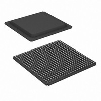
XC3S1600E-4FGG484I Xilinx Inc, XC3S1600E-4FGG484I Datasheet - Page 155

XC3S1600E-4FGG484I
Manufacturer Part Number
XC3S1600E-4FGG484I
Description
FPGA Spartan®-3E Family 1.6M Gates 33192 Cells 572MHz 90nm (CMOS) Technology 1.2V 484-Pin FBGA
Manufacturer
Xilinx Inc
Series
Spartan™-3Er
Datasheet
1.XC3S100E-4VQG100C.pdf
(233 pages)
Specifications of XC3S1600E-4FGG484I
Package
484FBGA
Family Name
Spartan®-3E
Device Logic Cells
33192
Device Logic Units
3688
Device System Gates
1600000
Number Of Registers
29504
Maximum Internal Frequency
572 MHz
Typical Operating Supply Voltage
1.2 V
Maximum Number Of User I/os
376
Ram Bits
663552
Number Of Logic Elements/cells
33192
Number Of Labs/clbs
3688
Total Ram Bits
663552
Number Of I /o
376
Number Of Gates
1600000
Voltage - Supply
1.14 V ~ 1.26 V
Mounting Type
Surface Mount
Operating Temperature
-40°C ~ 100°C
Package / Case
484-BBGA
Lead Free Status / RoHS Status
Lead free / RoHS Compliant
For Use With
HW-XA3S1600E-UNI-G - KIT DEVELOPMENT AUTOMOTIVE ECU
Lead Free Status / RoHS Status
Lead free / RoHS Compliant
Available stocks
Company
Part Number
Manufacturer
Quantity
Price
Company:
Part Number:
XC3S1600E-4FGG484I
Manufacturer:
XILINX
Quantity:
140
Company:
Part Number:
XC3S1600E-4FGG484I
Manufacturer:
XILINX
Quantity:
250
Company:
Part Number:
XC3S1600E-4FGG484I
Manufacturer:
Xilinx Inc
Quantity:
10 000
Part Number:
XC3S1600E-4FGG484I
Manufacturer:
XILINX/赛灵思
Quantity:
20 000
Table 117: Timing for the Slave Parallel Configuration Mode (Continued)
DS312-3 (v3.8) August 26, 2009
Product Specification
Notes:
1.
2.
3.
Hold Times
T
T
T
Clock Timing
T
T
F
SMCCD
SMCCCS
SMWCC
CCH
CCL
CCPAR
Symbol
The numbers in this table are based on the operating conditions set forth in
In the Slave Parallel mode, it is necessary to use the BUSY pin when the CCLK frequency exceeds this maximum specification.
Some Xilinx documents refer to Parallel modes as “SelectMAP” modes.
R
The time from the active edge of the CCLK pin to the point when data is last
held at the D0-D7 pins
The time from the active edge of the CCLK pin to the point when a logic level
is last held at the CSO_B pin
The time from the active edge of the CCLK pin to the point when a logic level
is last held at the RDWR_B pin
The High pulse width at the CCLK input pin
The Low pulse width at the CCLK input pin
Frequency of the clock
signal at the CCLK input
pin
No bitstream
compression
With bitstream compression
Description
www.xilinx.com
Not using the BUSY pin
Using the BUSY pin
Table
77.
DC and Switching Characteristics
(2)
All Speed Grades
Min
1.0
0
0
5
5
0
0
0
Max
50
66
20
-
-
-
-
-
Units
MHz
MHz
MHz
ns
ns
ns
ns
ns
155


