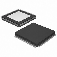
XC3S250E-4PQG208C Xilinx Inc, XC3S250E-4PQG208C Datasheet - Page 61

XC3S250E-4PQG208C
Manufacturer Part Number
XC3S250E-4PQG208C
Description
FPGA Spartan®-3E Family 250K Gates 5508 Cells 572MHz 90nm (CMOS) Technology 1.2V 208-Pin PQFP
Manufacturer
Xilinx Inc
Series
Spartan™-3Er
Datasheet
1.XC3S100E-4VQG100C.pdf
(233 pages)
Specifications of XC3S250E-4PQG208C
Package
208PQFP
Family Name
Spartan®-3E
Device Logic Cells
5508
Device Logic Units
612
Device System Gates
250000
Number Of Registers
4896
Maximum Internal Frequency
572 MHz
Typical Operating Supply Voltage
1.2 V
Maximum Number Of User I/os
158
Ram Bits
221184
Number Of Logic Elements/cells
5508
Number Of Labs/clbs
612
Total Ram Bits
221184
Number Of I /o
158
Number Of Gates
250000
Voltage - Supply
1.14 V ~ 1.26 V
Mounting Type
Surface Mount
Operating Temperature
0°C ~ 85°C
Package / Case
208-BFQFP
Lead Free Status / RoHS Status
Lead free / RoHS Compliant
Other names
122-1483
Available stocks
Company
Part Number
Manufacturer
Quantity
Price
Company:
Part Number:
XC3S250E-4PQG208C
Manufacturer:
XILINX
Quantity:
295
Company:
Part Number:
XC3S250E-4PQG208C
Manufacturer:
Xilinx Inc
Quantity:
10 000
Part Number:
XC3S250E-4PQG208C
Manufacturer:
XILINX/赛灵思
Quantity:
20 000
Part Number:
XC3S250E-4PQG208CS1
Manufacturer:
XILINX/赛灵思
Quantity:
20 000
By contrast, the clock switch matrixes on the top and bottom
edges receive signals from any of the five following sources:
two GCLK pins, two DCM outputs, or one Double-Line inter-
connect.
Table 41
inputs and BUFGMUX elements. The I0-input provides the
best input path to a clock buffer. The I1-input provides the
secondary input for the clock multiplexer function.
Table 41: Connections from Clock Inputs to BUFGMUX Elements and Associated Quadrant Clock
The connections for the bottom-edge BUFGMUX elements
are similar to the top-edge connections (see
DS312-2 (v3.8) August 26, 2009
Product Specification
Notes:
1.
2.
Quadrant
Line
Clock
See
See
within a quadrant.
G
H
E
D
C
B
A
F
(1)
Quadrant Clock Routing
Figure 45
indicates permissible connections between clock
R
Location
X0Y9
X0Y8
X0Y7
X0Y6
X0Y5
X0Y4
X0Y3
X0Y2
for specific BUFGMUX locations, and
Left-Half BUFGMUX
(2)
LHCLK7
LHCLK6
LHCLK5
LHCLK4
LHCLK3
LHCLK2
LHCLK1
LHCLK0
I0 Input
for connectivity details for the eight quadrant clocks.
LHCLK6
LHCLK7
LHCLK4
LHCLK5
LHCLK2
LHCLK3
LHCLK0
LHCLK1
I1 Input
Figure
Figure 47
Location
X1Y10
X1Y11
X2Y10
X2Y11
46).
X1Y0
X1Y1
X2Y0
X2Y1
Top or Bottom BUFGMUX
www.xilinx.com
(2)
for information on how BUFGMUX elements drive onto a specific clock line
GCLK7 or
GCLK6 or
GCLK5 or
GCLK4 or
GCLK3 or
GCLK2 or
GCLK1 or
GCLK0 or
The four BUFGMUX elements on the top edge are paired
together and share inputs from the eight global clock inputs
along the top edge. Each BUFGMUX pair connects to four
of the eight global clock inputs, as shown in
optionally allows differential inputs to the global clock inputs
without wasting a BUFGMUX element.
GCLK11
GCLK10
GCLK15
GCLK14
GCLK13
GCLK12
On the left and right edges, only two clock inputs feed each
pair of BUFGMUX elements.
I0 Input
GCLK9
GCLK8
GCLK6 or
GCLK7 or
GCLK4 or
GCLK5 or
GCLK2 or
GCLK3 or
GCLK0 or
GCLK1 or
GCLK10
GCLK11
GCLK14
GCLK15
GCLK12
GCLK13
I1 Input
GCLK8
GCLK9
Location
X3Y9
X3Y8
X3Y7
X3Y6
X3Y5
X3Y4
X3Y3
X3Y2
Right-Half BUFGMUX
(2)
Functional Description
RHCLK3
RHCLK2
RHCLK1
RHCLK0
RHCLK7
RHCLK6
RHCLK5
RHCLK4
I0 Input
Figure
RHCLK2
RHCLK3
RHCLK0
RHCLK1
RHCLK6
RHCLK7
RHCLK4
RHCLK5
I1 Input
45. This
61


