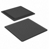
XC3SD1800A-4FG676I Xilinx Inc, XC3SD1800A-4FG676I Datasheet - Page 15

XC3SD1800A-4FG676I
Manufacturer Part Number
XC3SD1800A-4FG676I
Description
FPGA Spartan®-3A Family 1.8M Gates 37440 Cells 667MHz 90nm Technology 1.2V 676-Pin FBGA
Manufacturer
Xilinx Inc
Series
Spartan™-3A DSPr
Datasheets
1.XC3S50A-4VQG100C.pdf
(7 pages)
2.XC3SD3400A-4FGG676C.pdf
(4 pages)
3.XC3SD3400A-4FGG676C.pdf
(101 pages)
Specifications of XC3SD1800A-4FG676I
Package
676FBGA
Family Name
Spartan®-3A
Device Logic Units
37440
Device System Gates
1800000
Maximum Internal Frequency
667 MHz
Typical Operating Supply Voltage
1.2 V
Maximum Number Of User I/os
519
Ram Bits
1548288
Number Of Logic Elements/cells
37440
Number Of Labs/clbs
4160
Total Ram Bits
1548288
Number Of I /o
519
Number Of Gates
1800000
Voltage - Supply
1.14 V ~ 1.26 V
Mounting Type
Surface Mount
Operating Temperature
-40°C ~ 100°C
Package / Case
676-BBGA
Lead Free Status / RoHS Status
Contains lead / RoHS non-compliant
For Use With
122-1574 - KIT DEVELOPMENT SPARTAN 3ADSP
Lead Free Status / RoHS Status
Contains lead / RoHS non-compliant
Available stocks
Company
Part Number
Manufacturer
Quantity
Price
Company:
Part Number:
XC3SD1800A-4FG676I
Manufacturer:
XilinxInc
Quantity:
3 000
Company:
Part Number:
XC3SD1800A-4FG676I
Manufacturer:
Xilinx Inc
Quantity:
10 000
Part Number:
XC3SD1800A-4FG676I
Manufacturer:
XILINX/赛灵思
Quantity:
20 000
Table 11: DC Characteristics of User I/Os Using
Single-Ended Standards
DS610 (v3.0) October 4, 2010
Product Specification
LVTTL
LVCMOS33
LVCMOS25
LVCMOS18
LVCMOS15
LVCMOS12
IOSTANDARD
Attribute
(3)
(3)
(3)
(3)
(3)
(3)
24
16
24
12
16
12
8
4
6
12
16
24
12
16
12
2
4
6
8
2
4
6
8
2
4
6
8
2
4
6
8
2
4
6
2
(5)
(5)
(5)
(5)
(5)
(5)
(5)
(5)
(5)
(mA)
Conditions
I
12
16
24
12
16
24
12
16
24
12
16
12
OL
2
4
6
8
2
4
6
8
2
4
6
8
2
4
6
8
2
4
6
8
2
4
6
Test
(mA)
–12
–16
–24
–12
–16
–24
–12
–16
–24
–12
–16
–12
I
–2
–4
–6
–8
–2
–4
–6
–8
–2
–4
–6
–8
–2
–4
–6
–8
–2
–4
–6
–8
–2
–4
–6
OH
Max (V)
V
0.4
0.4
0.4
0.4
0.4
0.4
Characteristics
OL
Logic Level
V
V
V
V
V
CCO
CCO
CCO
CCO
CCO
Min (V)
V
2.4
OH
Spartan-3A DSP FPGA Family: DC and Switching Characteristics
–
–
–
–
–
www.xilinx.com
0.4
0.4
0.4
0.4
0.4
Table 11: DC Characteristics of User I/Os Using
Single-Ended Standards (Cont’d)
Notes:
1.
2.
3.
4.
5.
PCI33_3
PCI66_3
HSTL_I
HSTL_III
HSTL_I_18
HSTL_II_18
HSTL_III_18
SSTL18_I
SSTL18_II
SSTL2_I
SSTL2_II
SSTL3_I
SSTL3_II
IOSTANDARD
The numbers in this table are based on the conditions set forth in
Table 7
Descriptions of the symbols used in this table are as follows:
I
I
V
V
V
V
For the LVCMOS and LVTTL standards: the same V
limits apply for the Fast, Slow, and QUIETIO slew attributes.
Tested according to the relevant PCI specifications. For
information on PCI IP solutions, see
design_resources/conn_central/protocols/pci_pcix.htm. The
PCIX IOSTANDARD is available and has equivalent
characteristics but no PCI-X IP is supported.
These higher-drive output standards are supported only on
FPGA banks 1 and 3. Inputs are unrestricted. See the Using I/O
Resources chapter in UG331.
OL
OH
OL
OH
CCO
TT
Attribute
—the output current condition under which VOL is tested
—the output current condition under which VOH is tested
—the voltage applied to a resistor termination
— the output voltage that indicates a Low logic level
—the output voltage that indicates a High logic level
(5)
(4)
(4)
—the supply voltage for output drivers
(5)
(5)
(5)
(5)
and
(5)
Table
10.
(mA)
Conditions
13.4 –13.4 V
16.2 –16.2
I
1.5
1.5
6.7
8.1
24
16
24
16
OL
8
8
8
Test
(mA)
–0.5
–0.5
–6.7
–8.1
–16
–16
I
–8
–8
–8
–8
–8
OH
V
10% V
10% V
www.xilinx.com/products/
V
V
V
V
TT
TT
Max (V)
TT
TT
TT
TT
V
0.4
0.4
0.4
0.4
0.4
–
–
Characteristics
–
–
OL
–
–
0.475 V
0.603 V
Logic Level
0.61
0.81
CCO
CCO
0.6
0.8
V
V
V
V
V
90% V
90% V
V
V
OL
V
V
TT
TT
CCO
CCO
CCO
CCO
CCO
Min (V)
TT
TT
TT
TT
V
and V
+ 0.475
+ 0.603
+ 0.61
+ 0.81
OH
+ 0.6
+ 0.8
–
–
–
–
–
CCO
CCO
0.4
0.4
0.4
0.4
0.4
OH
15


