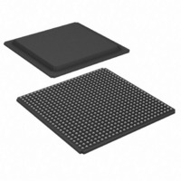
XC3SD1800A-4FG676I Xilinx Inc, XC3SD1800A-4FG676I Datasheet - Page 31

XC3SD1800A-4FG676I
Manufacturer Part Number
XC3SD1800A-4FG676I
Description
FPGA Spartan®-3A Family 1.8M Gates 37440 Cells 667MHz 90nm Technology 1.2V 676-Pin FBGA
Manufacturer
Xilinx Inc
Series
Spartan™-3A DSPr
Datasheets
1.XC3S50A-4VQG100C.pdf
(7 pages)
2.XC3SD3400A-4FGG676C.pdf
(4 pages)
3.XC3SD3400A-4FGG676C.pdf
(101 pages)
Specifications of XC3SD1800A-4FG676I
Package
676FBGA
Family Name
Spartan®-3A
Device Logic Units
37440
Device System Gates
1800000
Maximum Internal Frequency
667 MHz
Typical Operating Supply Voltage
1.2 V
Maximum Number Of User I/os
519
Ram Bits
1548288
Number Of Logic Elements/cells
37440
Number Of Labs/clbs
4160
Total Ram Bits
1548288
Number Of I /o
519
Number Of Gates
1800000
Voltage - Supply
1.14 V ~ 1.26 V
Mounting Type
Surface Mount
Operating Temperature
-40°C ~ 100°C
Package / Case
676-BBGA
Lead Free Status / RoHS Status
Contains lead / RoHS non-compliant
For Use With
122-1574 - KIT DEVELOPMENT SPARTAN 3ADSP
Lead Free Status / RoHS Status
Contains lead / RoHS non-compliant
Available stocks
Company
Part Number
Manufacturer
Quantity
Price
Company:
Part Number:
XC3SD1800A-4FG676I
Manufacturer:
XilinxInc
Quantity:
3 000
Company:
Part Number:
XC3SD1800A-4FG676I
Manufacturer:
Xilinx Inc
Quantity:
10 000
Part Number:
XC3SD1800A-4FG676I
Manufacturer:
XILINX/赛灵思
Quantity:
20 000
Table 25:
DS610 (v3.0) October 4, 2010
Product Specification
LVCMOS12
PCI33_3
PCI66_3
HSTL_I
HSTL_III
HSTL_I_18
HSTL_II_18
HSTL_III_18
SSTL18_I
SSTL18_II
SSTL2_I
SSTL2_II
SSTL3_I
SSTL3_II
LVCMOS25 with 12mA Drive
Following Signal Standard
Convert Output Time from
and Fast Slew Rate to the
(IOSTANDARD)
Output Timing Adjustments for IOB
QuietIO
Slow
Fast
2 mA
4 mA
6 mA
2 mA
4 mA
6 mA
2 mA
4 mA
6 mA
50.76
43.17
37.31
–0.05
Speed Grade
7.14
4.87
5.67
6.77
5.02
4.09
0.34
0.34
0.78
1.16
0.35
0.30
0.47
0.40
0.30
0.00
0.00
0.17
Adjustment
-5
Add the
Below
50.76
43.17
37.31
–0.05
7.14
4.87
5.67
6.77
5.02
4.09
0.34
0.34
0.78
1.16
0.35
0.30
0.47
0.40
0.30
0.00
0.00
0.17
-4
(Cont’d)
Units
Spartan-3A DSP FPGA Family: DC and Switching Characteristics
ns
ns
ns
ns
ns
ns
ns
ns
ns
ns
ns
ns
ns
ns
ns
ns
ns
ns
ns
ns
ns
ns
www.xilinx.com
Table 25:
Notes:
1.
2.
3.
Differential Standards
LVDS_25
LVDS_33
BLVDS_25
MINI_LVDS_25
MINI_LVDS_33
LVPECL_25
LVPECL_33
RSDS_25
RSDS_33
TMDS_33
PPDS_25
PPDS_33
DIFF_HSTL_I_18
DIFF_HSTL_II_18
DIFF_HSTL_III_18
DIFF_HSTL_I
DIFF_HSTL_III
DIFF_SSTL18_I
DIFF_SSTL18_II
DIFF_SSTL2_I
DIFF_SSTL2_II
DIFF_SSTL3_I
DIFF_SSTL3_II
LVCMOS25 with 12mA Drive
Following Signal Standard
Convert Output Time from
and Fast Slew Rate to the
The numbers in this table are tested using the methodology
presented in
set forth in
These adjustments are used to convert output- and
three-state-path times originally specified for the LVCMOS25
standard with 12 mA drive and Fast slew rate to times that
correspond to other signal standards. Do not adjust times that
measure when outputs go into a high-impedance state.
Note that 16 mA drive is faster than 24 mA drive for the Slow
slew rate.
(IOSTANDARD)
Output Timing Adjustments for IOB
Table
Table 26
7,
Table
and are based on the operating conditions
10, and
Table
Speed Grade
1.16
0.46
0.11
0.75
0.40
1.42
0.58
0.46
1.07
0.63
0.43
0.41
0.36
1.01
0.54
0.49
0.41
0.82
0.09
1.16
0.28
Adjustment
-5
Add the
12.
Below
Inputs Only
1.16
0.46
0.11
0.75
0.40
1.42
0.58
0.46
1.07
0.63
0.43
0.41
0.36
1.01
0.54
0.49
0.41
0.82
0.09
1.16
0.28
-4
(Cont’d)
Units
ns
ns
ns
ns
ns
ns
ns
ns
ns
ns
ns
ns
ns
ns
ns
ns
ns
ns
ns
ns
ns
31


