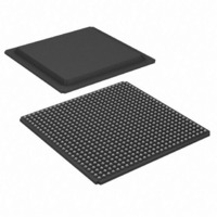
XC3SD1800A-4FG676I Xilinx Inc, XC3SD1800A-4FG676I Datasheet - Page 72

XC3SD1800A-4FG676I
Manufacturer Part Number
XC3SD1800A-4FG676I
Description
FPGA Spartan®-3A Family 1.8M Gates 37440 Cells 667MHz 90nm Technology 1.2V 676-Pin FBGA
Manufacturer
Xilinx Inc
Series
Spartan™-3A DSPr
Datasheets
1.XC3S50A-4VQG100C.pdf
(7 pages)
2.XC3SD3400A-4FGG676C.pdf
(4 pages)
3.XC3SD3400A-4FGG676C.pdf
(101 pages)
Specifications of XC3SD1800A-4FG676I
Package
676FBGA
Family Name
Spartan®-3A
Device Logic Units
37440
Device System Gates
1800000
Maximum Internal Frequency
667 MHz
Typical Operating Supply Voltage
1.2 V
Maximum Number Of User I/os
519
Ram Bits
1548288
Number Of Logic Elements/cells
37440
Number Of Labs/clbs
4160
Total Ram Bits
1548288
Number Of I /o
519
Number Of Gates
1800000
Voltage - Supply
1.14 V ~ 1.26 V
Mounting Type
Surface Mount
Operating Temperature
-40°C ~ 100°C
Package / Case
676-BBGA
Lead Free Status / RoHS Status
Contains lead / RoHS non-compliant
For Use With
122-1574 - KIT DEVELOPMENT SPARTAN 3ADSP
Lead Free Status / RoHS Status
Contains lead / RoHS non-compliant
Available stocks
Company
Part Number
Manufacturer
Quantity
Price
Company:
Part Number:
XC3SD1800A-4FG676I
Manufacturer:
XilinxInc
Quantity:
3 000
Company:
Part Number:
XC3SD1800A-4FG676I
Manufacturer:
Xilinx Inc
Quantity:
10 000
Part Number:
XC3SD1800A-4FG676I
Manufacturer:
XILINX/赛灵思
Quantity:
20 000
User I/Os by Bank
Table 64
The AWAKE pin is counted as a dual-purpose I/O.
Table 64: User I/Os Per Bank for the XC3SD1800A in the CS484 Package
Table 65: User I/Os Per Bank for the XC3SD3400A in the CS484 Package
Footprint Migration Differences
There are no migration footprint differences between the XC3SD1800A and the XC3SD3400A in the CS484 package.
DS610 (v3.0) October 4, 2010
Product Specification
Notes:
1.
Notes:
1.
Top
Right
Bottom
Left
Top
Right
Bottom
Left
Package
Package
TOTAL
19 VREF are on INPUT pins.
TOTAL
19 VREF are on INPUT pins.
Edge
Edge
and
Table 65
I/O Bank
I/O Bank
0
1
2
3
0
1
2
3
indicates how the user-I/O pins are distributed between the four I/O banks on the CS484 package.
Maximum I/Os
Maximum I/O
Input-Only
Input-Only
and
and
309
309
77
78
76
78
77
78
76
78
156
156
I/O
I/O
49
23
33
51
49
23
33
51
www.xilinx.com
INPUT
INPUT
Spartan-3A DSP FPGA Family: Pinout Descriptions
13
13
41
13
13
41
9
6
9
6
All Possible I/O Pins by Type
All Possible I/O Pins by Type
DUAL
DUAL
30
21
52
30
21
52
1
0
1
0
VREF
VREF
28
28
6
8
8
6
6
8
8
6
(1)
(1)
CLK
CLK
32
32
8
8
8
8
8
8
8
8
72


