PIMD2,125 NXP Semiconductors, PIMD2,125 Datasheet
PIMD2,125
Specifications of PIMD2,125


Related parts for PIMD2,125


PIMD2,125 Summary of contents
Page 1
PEMD2; PIMD2; PUMD2 NPN/PNP resistor-equipped transistors Rev. 07 — 24 September 2008 1. Product profile 1.1 General description NPN/PNP Resistor-Equipped Transistors (RET). Table 1. Type number PEMD2 PIMD2 PUMD2 1.2 Features ...
Page 2
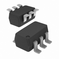
... NXP Semiconductors 2. Pinning information Table 3. Pin PEMD2; PUMD2 PIMD2 Ordering information Table 4. Type number PEMD2 PIMD2 PUMD2 PEMD2_PIMD2_PUMD2_7 Product data sheet PEMD2; PIMD2; PUMD2 NPN/PNP resistor-equipped transistors Pinning Description GND (emitter) TR1 input (base) TR1 output (collector) TR2 GND (emitter) TR2 ...
Page 3
... NXP Semiconductors 4. Marking Table 5. Type number PEMD2 PIMD2 PUMD2 [ made in Hong Kong * = p: made in Hong Kong * = t: made in Malaysia * = W: made in China 5. Limiting values Table 6. In accordance with the Absolute Maximum Rating System (IEC 60134). Symbol Per transistor; for the PNP transistor with negative polarity ...
Page 4
... NXP Semiconductors Table 6. In accordance with the Absolute Maximum Rating System (IEC 60134). Symbol Per device P tot [1] Device mounted on an FR4 Printed-Circuit Board (PCB), single-sided copper, tin-plated and standard footprint. [2] Reflow soldering is the only recommended soldering method. 6. Thermal characteristics Table 7. ...
Page 5
... NXP Semiconductors 7. Characteristics Table unless otherwise specified. amb Symbol Per transistor; for the PNP transistor with negative polarity I CBO I CEO I EBO CEsat V I(off) V I(on) R1 R2/ PEMD2_PIMD2_PUMD2_7 Product data sheet PEMD2; PIMD2; PUMD2 NPN/PNP resistor-equipped transistors Characteristics Parameter Conditions collector-base cut-off ...
Page 6
... NXP Semiconductors (1) ( 150 C amb ( amb ( amb Fig 1. TR1 (NPN): DC current gain as a function of collector current; typical values 10 V I(on) (V) (1) ( amb ( amb ( 100 C amb Fig 3. TR1 (NPN): On-state input voltage as a function of collector current; typical values PEMD2_PIMD2_PUMD2_7 Product data sheet PEMD2 ...
Page 7
... NXP Semiconductors (1) T (2) T (3) T Fig 5. PEMD2_PIMD2_PUMD2_7 Product data sheet PEMD2; PIMD2; PUMD2 NPN/PNP resistor-equipped transistors CEsat ( ) 100 C amb = 25 C amb = 40 C amb TR1 (NPN): Collector-emitter saturation resistance as a function of collector current; typical values Rev. 07 — 24 September 2008 006aab351 (1) (2) ( (mA) C © ...
Page 8
... NXP Semiconductors (1) FE ( 150 C amb ( amb ( amb Fig 6. TR2 (PNP): DC current gain as a function of collector current; typical values 10 V I(on) (V) (1) ( amb ( amb ( 100 C amb Fig 8. TR2 (PNP): On-state input voltage as a function of collector current; typical values PEMD2_PIMD2_PUMD2_7 Product data sheet PEMD2 ...
Page 9
... NXP Semiconductors (1) T (2) T (3) T Fig 10. TR2 (PNP): Collector-emitter saturation resistance as a function of collector PEMD2_PIMD2_PUMD2_7 Product data sheet PEMD2; PIMD2; PUMD2 NPN/PNP resistor-equipped transistors CEsat ( ) 100 C amb = 25 C amb = 40 C amb current; typical values Rev. 07 — 24 September 2008 006aab352 (1) (2) ( (mA) C © ...
Page 10
... NXP Semiconductors 8. Package outline 1.7 1 1.7 1.3 1.5 1.1 pin 1 index 1 2 0.5 1 Dimensions in mm Fig 11. Package outline PEMD2 (SOT666) Fig 13. Package outline PUMD2 (SOT363/SC-88) PEMD2_PIMD2_PUMD2_7 Product data sheet PEMD2; PIMD2; PUMD2 NPN/PNP resistor-equipped transistors 0.6 0.5 4 0.3 0.1 3.0 2 ...
Page 11
... NXP Semiconductors 9. Packing information Table 9. The indicated -xxx are the last three digits of the 12NC ordering code. Type number Package Description PEMD2 PIMD2 PUMD2 [1] For further information and the availability of packing methods, see [2] T1: normal taping [3] T2: reverse taping 10. Soldering 2 1.7 Fig 14. Refl ...
Page 12
... NXP Semiconductors 3.3 Fig 15. Reflow soldering footprint PIMD2 (SOT457/SC-74) 1.475 5.05 1.475 Fig 16. Wave soldering footprint PIMD2 (SOT457/SC-74) PEMD2_PIMD2_PUMD2_7 Product data sheet PEMD2; PIMD2; PUMD2 NPN/PNP resistor-equipped transistors 3.45 1.95 0.95 2.825 0. 2.4 5.3 1. 2.85 Rev. 07 — 24 September 2008 ...
Page 13
... NXP Semiconductors Fig 17. Reflow soldering footprint PUMD2 (SOT363/SC-88) 4.5 Fig 18. Wave soldering footprint PUMD2 (SOT363/SC-88) PEMD2_PIMD2_PUMD2_7 Product data sheet PEMD2; PIMD2; PUMD2 NPN/PNP resistor-equipped transistors 2.65 1.5 2.35 0 1.8 1.3 1.3 2.45 5.3 Rev. 07 — 24 September 2008 0 0.6 ...
Page 14
... NPN/PNP resistor-equipped transistors Data sheet status Product data sheet The format of this data sheet has been redesigned to comply with the new identity guidelines of NXP Semiconductors. Legal texts have been adapted to the new company name where appropriate. Table 8 “Characteristics”: V unit corrected ...
Page 15
... Right to make changes — NXP Semiconductors reserves the right to make changes to information published in this document, including without limitation specifications and product descriptions, at any time and without notice ...
Page 16
... NXP Semiconductors 14. Contents 1 Product profi 1.1 General description 1.2 Features . . . . . . . . . . . . . . . . . . . . . . . . . . . . . . 1 1.3 Applications . . . . . . . . . . . . . . . . . . . . . . . . . . . 1 1.4 Quick reference data Pinning information . . . . . . . . . . . . . . . . . . . . . . 2 3 Ordering information . . . . . . . . . . . . . . . . . . . . . 2 4 Marking . . . . . . . . . . . . . . . . . . . . . . . . . . . . . . . . 3 5 Limiting values Thermal characteristics Characteristics . . . . . . . . . . . . . . . . . . . . . . . . . . 5 8 Package outline . . . . . . . . . . . . . . . . . . . . . . . . 10 9 Packing information Soldering . . . . . . . . . . . . . . . . . . . . . . . . . . . . . 11 11 Revision history . . . . . . . . . . . . . . . . . . . . . . . . 14 12 Legal information ...