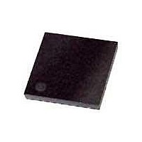
ATA5823-PLQW80 Atmel, ATA5823-PLQW80 Datasheet - Page 27

ATA5823-PLQW80
Manufacturer Part Number
ATA5823-PLQW80
Description
RF Transceiver RF Data Control Duplex Transceiver
Manufacturer
Atmel
Datasheet
1.ATA5824-PLQW.pdf
(98 pages)
Specifications of ATA5823-PLQW80
Output Power
10 dBm
Operating Supply Voltage
2.15 V to 3.6 V
Maximum Operating Temperature
+ 105 C
Mounting Style
SMD/SMT
Package / Case
QFN-48
Minimum Operating Temperature
- 40 C
Modulation
ASK, FSK
Lead Free Status / RoHS Status
Lead free / RoHS Compliant
9. XTO
4829D–RKE–06/06
Table 8-2.
Table 8-3.
The XTO is an amplitude regulated Pierce oscillator type with integrated load capacitances
(2
lation frequency f
designing the system in terms of receiving and transmitting frequency offset the accuracy of the
crystal and XTO have to be considered.
The synthesizer can adjust the local oscillator frequency for the initial frequency error in f
This is done at nominal supply voltage and temperature with the control registers 2 and 3 (see
Table 12-7 on page 38
nominal supply voltage and temperature is then < ±0.5 ppm. The XTO’s gm has very low influ-
ence of less than ±2 ppm on the frequency at nominal supply voltage and temperature.
In a single channel system less than ±150 ppm should be corrected to avoid that harmonics of
the CLK output disturb the receive mode. If the CLK is not used, or carefully layouted on the
application PCB (as needed for multi channel systems), more than ±150 ppm can be
compensated.
The additional XTO pulling is only ±2 ppm, overtemperature and supply voltage. The XTAL ver-
sus temperature and its aging is then the main source of frequency error in the local oscillator.
The XTO frequency depends on XTAL properties and the load capacitances C
and XTAL2. The pulling of f
C
found in its datasheet. C
sists of C
P
m
=
is the crystal's motional, C
V
18 pF with a tolerance of ±17%) hence C
C
------- -
S
2
m
V
= V
T
T
T
S
T
T
T
amb
amb
L1
amb
amb
amb
amb
= V
S1
------------------------------------------------------------ -
C
and C
= +105°C
= +105°C
= V
= –40°C
= +25°C
= –40°C
= +25°C
S2
0
+
Typical Measured Supply Current and Output Power in Full-duplex Mode
433.92 MHz/Power Amplifier is Load Optimized for +5 dBm, R
PWRSET = 20, (Battery Application)
Typical Measured Supply Current and Output Power in Full-duplex Mode/
433.92 MHz/Power Amplifier is Load Optimized for +5 dBm, R
PWRSET = 31, (Car Application)
= V
S2
C
C
LN
L2
= V
XTO
SINT
LN
in series connection.
SINT
–
is the reference frequency FREF for the fractional-N synthesizer. When
C
and
C
L
L
0
is the total actual load capacitance of the crystal in the circuit and con-
+
XTO
Table 12-10 on page
C
L
0
13.4 mA/–7.5 dBm
from the nominal f
10.2 mA/–6.2 dBm
11.8 mA/–6.4 dBm
17.6 mA/ 4.6 dBm
13.6 mA/3.7 dBm
15.6 mA/4.3 dBm
the shunt and C
10
6
2.15V
4.4V
ppm.
Lmin
39). The remaining local oscillator tolerance at
XTAL
LN
= 7.4 pF and C
the nominal load capacitance of the XTAL
10.9 mA/–5.2 dBm
12.5 mA/–5.2 dBm
14.2 mA/–5.9 dBm
is calculated using the following formula:
13.6 mA/3.7 dBm
15.6 mA/4.3 dBm
17.6 mA/4.6 dBm
ATA5823/ATA5824
3.0V
5V
Lmax
= 10.6 pF. The XTO oscil-
11.4 mA/–4.6 dBm
13.1 mA/–4.5 dBm
14.8 mA/–5.0 dBm
1
1
13.6 mA/3.7 dBm
15.6 mA/4.3 dBm
17.6 mA/4.6 dBm
= 22k,
= 22k,
L1, 2
5.25V
3.6V
at pin XTAL1
XTO
27
.


