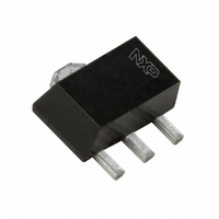
PBSS306PX,115 NXP Semiconductors, PBSS306PX,115 Datasheet - Page 11

PBSS306PX,115
Manufacturer Part Number
PBSS306PX,115
Description
TRANS PNP 100V 3.7A SOT-89
Manufacturer
NXP Semiconductors
Series
-r
Datasheet
1.PBSS306PX115.pdf
(15 pages)
Specifications of PBSS306PX,115
Package / Case
SC-62, SOT-89, TO-243 (3 Leads + Tab)
Transistor Type
PNP
Current - Collector (ic) (max)
3.7A
Voltage - Collector Emitter Breakdown (max)
100V
Vce Saturation (max) @ Ib, Ic
300mV @ 400mA, 4A
Dc Current Gain (hfe) (min) @ Ic, Vce
100 @ 2A, 2V
Power - Max
2.1W
Frequency - Transition
100MHz
Mounting Type
Surface Mount
Minimum Operating Temperature
- 65 C
Configuration
Single
Transistor Polarity
PNP
Mounting Style
SMD/SMT
Collector- Emitter Voltage Vceo Max
100 V
Emitter- Base Voltage Vebo
5 V
Maximum Dc Collector Current
3.7 A
Power Dissipation
2100 mW
Maximum Operating Frequency
100 MHz
Maximum Operating Temperature
+ 150 C
Current - Collector Cutoff (max)
-
Lead Free Status / RoHS Status
Lead free / RoHS Compliant
Current - Collector Cutoff (max)
-
Lead Free Status / Rohs Status
Lead free / RoHS Compliant
Other names
934059019115
PBSS306PX T/R
PBSS306PX T/R
PBSS306PX T/R
PBSS306PX T/R
NXP Semiconductors
11. Soldering
PBSS306PX_2
Product data sheet
Fig 16. Reflow soldering footprint
Fig 17. Wave soldering footprint
4.60
0.85
SOT89 standard mounting conditions for reflow soldering
Not recommended for wave soldering
1.20
1.20
1.00
0.20
(3x)
1.50
3
Rev. 02 — 11 December 2009
6.60
2.40
0.70
5.30
3
3.70
1.90
1.20
3.95
4.75
2.25
2.00
2
1
2
0.50
100 V, 3.7 A PNP low V
1.20
3.50
3.00
1
0.60 (3x)
0.70 (3x)
7.60
0.50
preferred transport direction during soldering
1.20
1.70
4.85
Dimensions in mm
msa442
PBSS306PX
CEsat
solder lands
solder resist
occupied area
Dimensions in mm
© NXP B.V. 2009. All rights reserved.
(BISS) transistor
solder lands
solder resist
occupied area
solder paste
msa423
11 of 15


