IDT5T93GL161PFI IDT, Integrated Device Technology Inc, IDT5T93GL161PFI Datasheet
IDT5T93GL161PFI
Specifications of IDT5T93GL161PFI


Related parts for IDT5T93GL161PFI


IDT5T93GL161PFI Summary of contents
Page 1
LVDS, 1:16 GLITCHLESS CLOCK BUFFER TERABUFFER™ II General Description The IDT5T93GL161 2.5V differential clock buffer is a user-selectable differential input to sixteen LVDS outputs. The fanout from a differential input to sixteen LVDS outputs reduces loading on the preceding ...
Page 2
IDT5T93GL161 2.5V LVDS 1:16 GLITCHLESS CLOCK BUFFER TERABUFFER™ II Block Diagram SEL FSEL G2 IDT™ LVDS GLITCHLESS CLOCK BUFFER TERABUFFER™ OUTPUT CONTROL Q1 Q2 OUTPUT CONTROL Q2 Q3 OUTPUT ...
Page 3
IDT5T93GL161 2.5V LVDS 1:16 GLITCHLESS CLOCK BUFFER TERABUFFER™ II Table 1. Pin Descriptions Name Type A[1:2] Input Adjustable A[1:2] Input Adjustable G1 Input LVTTL G2 Input LVTTL GL Input LVTTL Q[1:16] Output LVDS Q{1:16} Output LVDS SEL Input LVTTL PD ...
Page 4
IDT5T93GL161 2.5V LVDS 1:16 GLITCHLESS CLOCK BUFFER TERABUFFER™ II Function Tables Table 3A. Gate Control Output Table Control Outputs GL G Q[1:16 Toggling 0 1 LOW 1 0 Toggling 1 1 HIGH Table 3B. Input Selection Table Selection ...
Page 5
IDT5T93GL161 2.5V LVDS 1:16 GLITCHLESS CLOCK BUFFER TERABUFFER™ II Absolute Maximum Ratings NOTE: Stresses beyond those listed under Absolute Maximum Ratings may cause permanent damage to the device. These ratings are stress specifications only. Functional operation of product at these ...
Page 6
IDT5T93GL161 2.5V LVDS 1:16 GLITCHLESS CLOCK BUFFER TERABUFFER™ II Table 4B. LVTTL DC Characteristics Symbol Parameter I Input High Current IH I Input Low Current IL V Clamp Diode Voltage Input Voltage Input High ...
Page 7
IDT5T93GL161 2.5V LVDS 1:16 GLITCHLESS CLOCK BUFFER TERABUFFER™ II Table 4D. LVDS DC Characteristics Symbol Parameter Differential Output Voltage for the V OT(+) True Binary State Differential Output Voltage for the V OT(–) False Binary State Change in V Between ...
Page 8
IDT5T93GL161 2.5V LVDS 1:16 GLITCHLESS CLOCK BUFFER TERABUFFER™ II Table 5B. eHSTL AC Differential Input Characteristics, T Symbol Parameter (1) V Input Signal Swing DIF V Differential Input Signal Crossing Point X D Duty Cycle H V Input Timing Measurement ...
Page 9
IDT5T93GL161 2.5V LVDS 1:16 GLITCHLESS CLOCK BUFFER TERABUFFER™ II Table 5E. AC Differential Input Characteristics Symbol Parameter ( Differential Voltage DIF V Differential Input Cross Point Voltage IX V Common Mode Input Voltage Range CM V Input Voltage ...
Page 10
IDT5T93GL161 2.5V LVDS 1:16 GLITCHLESS CLOCK BUFFER TERABUFFER™ II Differential AC Timing Waveforms Output Propagation and Skew Waveforms 1/ [1:2] [1:2] t PLH SK( NOTE 1: Pulse skew is calculated ...
Page 11
IDT5T93GL161 2.5V LVDS 1:16 GLITCHLESS CLOCK BUFFER TERABUFFER™ II Glitchless Output Operation with Switching Input Clock Selection SEL When SEL changes, the output clock goes LOW ...
Page 12
IDT5T93GL161 2.5V LVDS 1:16 GLITCHLESS CLOCK BUFFER TERABUFFER™ II FSEL Operation for When Opposite Clock Dies 1. When the differential on the non-selected clock goes below the minimum DC differential, the outputs clock goes to an unknown state. When this ...
Page 13
IDT5T93GL161 2.5V LVDS 1:16 GLITCHLESS CLOCK BUFFER TERABUFFER™ II Power Down Timing NOTE recommended that outputs be disabled before entering power-down mode. ...
Page 14
IDT5T93GL161 2.5V LVDS 1:16 GLITCHLESS CLOCK BUFFER TERABUFFER™ II Test Circuits and Conditions Test Circuit for Differential Input Pulse Generator Table 6A. Differential Input Test Conditions Symbol V = 2.5V ± 0. Crossing of A and A THI ...
Page 15
IDT5T93GL161 2.5V LVDS 1:16 GLITCHLESS CLOCK BUFFER TERABUFFER™ II Test Circuit for DC Outputs and Power Down Tests V A Pulse Generator D.U.T. A Test Circuit for Propagation, Skew, and Gate Enable/Disable Timing A Pulse Generator D.U.T. A Table 6B. ...
Page 16
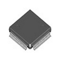
IDT5T93GL161 2.5V LVDS 1:16 GLITCHLESS CLOCK BUFFER TERABUFFER™ II Package Outline IDT™ LVDS GLITCHLESS CLOCK BUFFER TERABUFFER™ IDT5T93GL161 REV. A SEPTEMBER 12, 2008 ...
Page 17
IDT5T93GL161 2.5V LVDS 1:16 GLITCHLESS CLOCK BUFFER TERABUFFER™ II Package Dimensions IDT™ LVDS GLITCHLESS CLOCK BUFFER TERABUFFER™ IDT5T93GL161 REV. A SEPTEMBER 12, 2008 ...
Page 18
IDT5T93GL161 2.5V LVDS 1:16 GLITCHLESS CLOCK BUFFER TERABUFFER™ II Ordering Information Table 7. Ordering Information XX IDT XXXXX Package Device Type IDT™ LVDS GLITCHLESS CLOCK BUFFER TERABUFFER™ Process I PF PFG 5T93GL161 2.5V LVDS 1:16 Glitchless Clock Buffer ...
Page 19
IDT5T93GL161 2.5V LVDS 1:16 GLITCHLESS CLOCK BUFFER TERABUFFER™ II Revision History Sheet Rev Table Page Description of Change T3A 4 Added Gate Control Output Table. T3B 4 Added Selection Table Added Package Outline. 17 Added Package Dimensions. Updated ...
Page 20
IDT5T93GL161 2.5V LVDS 1:16 GLITCHLESS CLOCK BUFFER TERABUFFER™ II Contact Information: www.IDT.com Sales 800-345-7015 (inside USA) +408-284-8200 (outside USA) Fax: 408-284-2775 www.IDT.com/go/contactIDT © 2008 Integrated Device Technology, Inc. All rights reserved. Product specifications subject to change without notice. IDT and ...