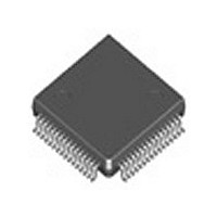
IDT5T93GL161PFI IDT, Integrated Device Technology Inc, IDT5T93GL161PFI Datasheet - Page 3

IDT5T93GL161PFI
Manufacturer Part Number
IDT5T93GL161PFI
Description
Manufacturer
IDT, Integrated Device Technology Inc
Type
Clock Driverr
Datasheet
1.IDT5T93GL161PFI.pdf
(20 pages)
Specifications of IDT5T93GL161PFI
Number Of Clock Inputs
2
Mode Of Operation
Differential
Output Frequency
450MHz
Output Logic Level
LVDS
Operating Supply Voltage (min)
2.3V
Operating Supply Voltage (typ)
2.5V
Operating Supply Voltage (max)
2.7V
Package Type
TQFP
Operating Temp Range
-40C to 85C
Operating Temperature Classification
Industrial
Mounting
Surface Mount
Pin Count
64
Quiescent Current
350mA
Lead Free Status / RoHS Status
Not Compliant
Table 1. Pin Descriptions
NOTES:
1.
2.
3.
4.
Table 2. Pin Characteristics
NOTE: This parameter is measured at characterization but not tested.
IDT™ LVDS GLITCHLESS CLOCK BUFFER TERABUFFER™ II
Symbol
C
IDT5T93GL161
2.5V LVDS 1:16 GLITCHLESS CLOCK BUFFER TERABUFFER™ II
IN
Q{1:16}
Inputs are capable of translating the following interface standards:
Single-ended 3.3V and 2.5V LVTTL levels
Differential HSTL and eHSTL levels
Differential LVEPECL (2.5V) and LVPECL (3.3V) levels
Differential LVDS levels
Differential CML levels
Because the gate controls are asynchronous, runt pulses are possible. It is the user's responsibility to either time the gate control
signals to minimize the possibility of runt pulses or be able to tolerate them in down stream circuitry.
It is recommended that the outputs be disabled before entering power-down mode. It is also recommended that the outputs remain
disabled until the device completes power-up after asserting PD.
The user must take precautions with any differential input interface standard being used in order to prevent instability when there is
no input signal.
Q[1:16]
Name
A[1:2]
A[1:2]
FSEL
GND
SEL
V
PD
G1
G2
GL
DD
Parameter
Input Capacitance
Output
Output
Input
Input
Input
Input
Input
Input
Input
Input
Adjustable
Adjustable
Type
LVTTL
LVTTL
LVTTL
LVTTL
LVTTL
LVTTL
Power
Power
LVDS
LVDS
(1, 4)
(1, 4)
(T
Description
Clock input. A
Complementary clock inputs. A[1:2] is the complementary side of A[1:2]
For LVTTL single-ended operation, A[1:2] should be set to the desired toggle
voltage for A[1:2]:
3.3V LVTTL V
2.5V LVTTL V
Gate control for differential outputs Q1 and Q1 through Q8 and Q8. When G1 is
LOW, the differential outputs are active. When G1 is HIGH, the differential
outputs are asynchronously driven to the level designated by GL
Gate control for differential outputs Q9 and Q9 through Q16 and Q16. When G2
is LOW, the differential outputs are active. When G2 is HIGH, the differential
outputs are asynchronously driven to the level designated by GL
Specifies output disable level. If HIGH, "true" outputs disable HIGH and
"complementary" outputs disable LOW. If LOW, "true" outputs disable LOW
and "complementary" outputs disable HIGH.
Clock outputs.
Complementary clock outputs.
Reference clock select. When LOW, selects A2 and A2.
When HIGH, selects A1 and A1.
Power-down control. Shuts off entire chip. If LOW, the device goes into LOW
power mode. Inputs and outputs are disabled. Both "true" and "complementary"
outputs will pull to V
At a rising edge, FSEL forces select to the input designated by SEL.
Set LOW for normal operation. At power-up, FSEL should be LOW.
Power supply for the device core and inputs.
Ground.
A
Test Conditions
= +25°C, F = 1.0MHz)
[1:2]
REF
REF
is the "true" side of the differential clock input.
= 1650mV
= 1250mV
DD
3
. Set HIGH for normal operation.
Minimum
IDT5T93GL161 REV. A SEPTEMBER 12, 2008
Typical
(3)
(2)
(2)
Maximum
.
.
3
.
Units
pF


