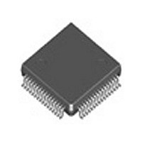
IDT5T93GL161PFI IDT, Integrated Device Technology Inc, IDT5T93GL161PFI Datasheet - Page 6

IDT5T93GL161PFI
Manufacturer Part Number
IDT5T93GL161PFI
Description
Manufacturer
IDT, Integrated Device Technology Inc
Type
Clock Driverr
Datasheet
1.IDT5T93GL161PFI.pdf
(20 pages)
Specifications of IDT5T93GL161PFI
Number Of Clock Inputs
2
Mode Of Operation
Differential
Output Frequency
450MHz
Output Logic Level
LVDS
Operating Supply Voltage (min)
2.3V
Operating Supply Voltage (typ)
2.5V
Operating Supply Voltage (max)
2.7V
Package Type
TQFP
Operating Temp Range
-40C to 85C
Operating Temperature Classification
Industrial
Mounting
Surface Mount
Pin Count
64
Quiescent Current
350mA
Lead Free Status / RoHS Status
Not Compliant
Table 4B. LVTTL DC Characteristics
NOTE 1: See Recommended Operating Range table.
NOTE 2: Typical values are at V
NOTE 3: For A[1:2] single-ended operation, A[1:2] is tied to a DC reference voltage.
Table 4C. Differential DC Characteristics
NOTE 1: See Recommended Operating Range table.
NOTE 2: V
V
input. The AC differential voltage must be achieved to guarantee switching to a new state.
NOTE 3: V
NOTE 4: Typical values are at V
IDT™ LVDS GLITCHLESS CLOCK BUFFER TERABUFFER™ II
Symbol
I
I
V
V
V
V
V
V
Symbol
I
I
V
V
V
V
CP
IH
IL
IH
IL
IDT5T93GL161
2.5V LVDS 1:16 GLITCHLESS CLOCK BUFFER TERABUFFER™ II
IK
IN
IH
IL
THI
REF
IK
IN
DIF
CM
is the "complement" input level. The DC differential voltage must be maintained to guarantee retaining the existing HIGH or LOW
DIF
CM
Parameter
Input High Current
Input Low Current
Clamp Diode Voltage
DC Input Voltage
DC Input High Voltage
DC Input Low Voltage
DC Input Threshold Crossing Voltage
Single-Ended Reference Voltage
Parameter
Input High Current
Input Low Current
Clamp Diode Voltage
DC Input Voltage
DC Differential Voltage
DC Common Mode Input Voltage
specifies the maximum allowable range of (V
specifies the minimum input differential voltage (V
DD
DD
= 2.5V, +25°C ambient.
= 2.5V, +25°C ambient.
(3)
(1)
, T
A
= -40°C to 85°C
(3)
(1)
, T
A
V
= -40°C to 85°C
V
DD
DD
Test Conditions
Test Conditions
TR
= 2.3V, I
V
V
= 2.3V, I
DD
DD
3.3V LVTTL
2.5V LVTTL
V
V
+ V
DD
DD
TR
= = 2.7V
= = 2.7V
CP
= 2.7V
= 2.7V
- V
IN
) /2.
6
IN
= -18mA
CP
= -18mA
) required for switching where V
Minimum
Minimum
0.05
-0.3
0.1
-0.3
1.7
IDT5T93GL161 REV. A SEPTEMBER 12, 2008
Typical
Typical
V
-0.7
1.65
1.25
-0.7
DD
TR
/2
(2)
is the "true" input level and
(2)
Maximum
Maximum
V
-1.2
-1.2
3.6
±5
±5
3.6
0.7
±5
±5
DD
Units
Units
µA
µA
µA
µA
V
V
V
V
V
V
V
V
V
V
V


