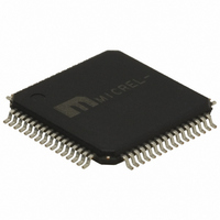
SY89221UHY Micrel Inc, SY89221UHY Datasheet

SY89221UHY
Specifications of SY89221UHY
Available stocks
Related parts for SY89221UHY
SY89221UHY Summary of contents
Page 1
... All support documentation can be found at Micrel's web site at: www.micrel.com. Precision Edge is a registered trademark of Micrel, Inc. Micrel Inc. • 2180 Fortune Drive • San Jose, CA 95131 • USA • tel +1 ( August 2007 Precision 1:15 LVPECL Fanout Buffer with 2:1 MUX and Four ÷1/÷2/÷4 Clock Divider Features • ...
Page 2
Functional Block Diagram August 2007 2 hbwhelp@micrel.com M9999-082407-C or (408) 955-1690 ...
Page 3
... Contact factory for die availability. Dice are guaranteed Tape and Reel. Pin Configuration August 2007 Operating Package Marking Type Range Industrial SY89221UHY with Pb-Free bar-line indicator SY89221UHY with T64-1 Industrial Pb-Free bar-line indicator = 25°C, DC Electricals only. A 64-Pin EPAD-TQFP (T64-1) 3 Lead Finish Pb-Free ...
Page 4
Pin Description Pin Number Pin Name 1, 2 FSELA1, FSELA0 3, 4 FSELB1, FSELB0 15, 16 FSELC1, FSELC0 17, 18 FSELD1, FSELD0 5, 8, IN0, /IN0 11, 14 IN1, /IN1 6, 12 VT0, VT1 7, VREF-AC0, 13 VREF-AC1 9 /MR ...
Page 5
Pin Description (continued) Pin Number Pin Name 64 EN 19, 32, 49, 63 GND, Exposed Pad Function Table (1) (2, 3) /MR EN CLK_SEL ...
Page 6
Absolute Maximum Ratings Supply Voltage (V ) ............................... –0.5V to +4.0V CC Input Voltage (V ) .......................................–0. Termination Current Source or sink current LVPECL Output Current (I ) OUT Continuous.......................................................50mA Surge .............................................................100mA Input Current ...
Page 7
LVTTL/CMOS DC Electrical Characteristics V = +2.5V ±5% or 3.3V ±10 Symbol Parameter V Input HIGH Voltage IH V Input LOW Voltage IL I Input HIGH Current IH I Input LOW Current IL LVPECL Outputs DC Electrical Characteristics ...
Page 8
AC Electrical Characteristics V = +2.5V ±5% or 3.3V ±10 Symbol Parameter f Maximum Operating Frequency MAX t Differential Propagation Delay PD t Reset Recovery Time RR t Differential Propagation Delay PD Tempco Temperature Coefficient t Within-Bank Skew ...
Page 9
Functional Description Clock Select (CLK_SEL) CLK_SEL is an asynchronous TTL/CMOS compatible input that selects one of the two input signals. Internal 25kΩ pull-up resistor defaults the input to logic HIGH if left open. Delay between the clock selection and multiplexer ...
Page 10
Single-Ended and Differential Swings Figure 1a. Single-Ended Voltage Swing Timing Diagrams August 2007 Figure 1b. Differential Voltage Swing Figure 2a. Propagation Delay Figure 2b. Fail Safe Feature 10 M9999-082407-C hbwhelp@micrel.com or (408) 955-1690 ...
Page 11
Micrel, Inc. Timing Diagrams August 2007 Figure 2c. Reset with Output Enabled 11 SY89221U M9999-082407-C hbwhelp@micrel.com or (408) 955-1690 ...
Page 12
Timing Diagrams August 2007 Figure 2d. Enable Timing Figure 2e. Disable Timing 12 M9999-082407-C hbwhelp@micrel.com or (408) 955-1690 ...
Page 13
Typical Operating Characteristics V = 3.3V, GND = 0V 100mV August 2007 = 50Ω -2V 25°C, unless otherwise stated M9999-082407-C hbwhelp@micrel.com or (408) 955-1690 ...
Page 14
Functional Characteristics V = 3.3V, GND = 0V 100mV August 2007 = 50Ω -2V 25°C, unless otherwise stated M9999-082407-C hbwhelp@micrel.com or (408) 955-1690 ...
Page 15
Input and Output Stages Figure 3a. Simplified Differential Input Stage Input Interface Applications Figure 4a. CML Interface (DC-Coupled) May connect Figure 4d. LVPECL Interface (AC-Coupled) August 2007 Figure 3b. Simplified Differential Output Stage Figure 4b. ...
Page 16
LVPECL Output Interface Applications LVPECL has high input impedance, and very low output impedance (open emitter), and small signal swing which results in low EMI. LVPECL is ideal for driving 50Ω- and 100Ω-controlled transmission lines. There are several techniques for ...
Page 17
Micrel, Inc. Package Information MICREL, INC. 2180 FORTUNE DRIVE SAN JOSE, CA 95131 USA TEL +1 (408) 944-0800 FAX +1 (408) 474-1000 WEB http:/www.micrel.com The information furnished by Micrel in this data sheet is believed to be accurate and reliable. ...


