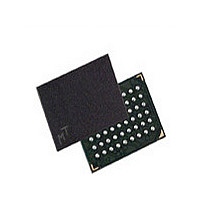
MT48H4M16LFB4-75 IT:H Micron Technology Inc, MT48H4M16LFB4-75 IT:H Datasheet - Page 11

MT48H4M16LFB4-75 IT:H
Manufacturer Part Number
MT48H4M16LFB4-75 IT:H
Description
Manufacturer
Micron Technology Inc
Type
SDRAMr
Datasheet
1.MT48H4M16LFB4-75_ITH.pdf
(62 pages)
Specifications of MT48H4M16LFB4-75 IT:H
Organization
4Mx16
Density
64Mb
Address Bus
14b
Maximum Clock Rate
133MHz
Operating Supply Voltage (typ)
1.8V
Package Type
VFBGA
Operating Temp Range
-40C to 85C
Operating Supply Voltage (max)
1.9V
Operating Supply Voltage (min)
1.7V
Supply Current
50mA
Pin Count
54
Mounting
Surface Mount
Operating Temperature Classification
Industrial
Lead Free Status / RoHS Status
Compliant
Figure 5:
Operating Mode
Write Burst Mode
Extended Mode Register
PDF: 09005aef8237ed98/Source: 09005aef8237ed68
64mb_x16_Mobile SDRAM_Y24L_2.fm - Rev. C 10/07 EN
CAS Latency
Command
Command
The normal operating mode is selected by setting M7 and M8 to zero; the other combi-
nations of values for M7 and M8 are reserved for future use. The programmed burst
length applies to both read and write bursts.
Reserved states must not be used; unknown operation or incompatibility with future
versions may result.
When M9 = 0, the burst length programmed via M0–M2 applies to both READ and
WRITE bursts; when M9 = 1, the programmed burst length applies to READ bursts, but
write accesses are single-location accesses.
The extended mode register controls the functions beyond those controlled by the mode
register. These additional functions are special features of the mobile device. They
include temperature-compensated self refresh (TCSR) control, partial-array self refresh
(PASR), and output drive strength.
The extended mode register is programmed via the MODE REGISTER SET command
with BA = 1 and BA = 0 and retains the stored information until it is programmed again
or the device loses power.
The extended mode register must be loaded when all banks are idle and no bursts are in
progress, and the controller must wait
Violating any of these requirements will result in unspecified operation.
CLK
CLK
DQ
DQ
READ
READ
T0
T0
CL = 2
NOP
NOP
T1
T1
t
t AC
LZ
CL = 3
11
T2
T2
NOP
NOP
t
t AC
LZ
D
t OH
OUT
t
MRD before initiating any subsequent operation.
Micron Technology, Inc., reserves the right to change products or specifications without notice.
64Mb: 4 Meg x 16 Mobile SDRAM
T3
T3
NOP
D
t OH
OUT
Don’t Care
Undefined
Mode Register Definition
T4
©2006 Micron Technology, Inc. All rights reserved.


