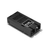
HFCT5201B Avago Technologies US Inc., HFCT5201B Datasheet - Page 3

HFCT5201B
Manufacturer Part Number
HFCT5201B
Description
Manufacturer
Avago Technologies US Inc.
Datasheet
1.HFCT5201B.pdf
(8 pages)
Specifications of HFCT5201B
Optical Fiber Type
TX/RX
Data Transfer Rate
155Mbps
Operating Temperature Classification
Commercial
Peak Wavelength
1360nm
Operating Supply Voltage (min)
4.75V
Operating Supply Voltage (typ)
5V
Operating Supply Voltage (max)
5.25V
Output Current
30mA
Operating Temp Range
0C to 70C
Pin Count
18
Lead Free Status / RoHS Status
Not Compliant
Figure 3. Relative Input Optical Power
- dBm. Avg.
plane printed circuit board is best
for distribution of V
ground currents, forming transmis‑
sion lines and shielding, Also, it is
important to suppress noise from
influencing the fiber‑optic trans‑
ceiver performance, especially the
receiver circuit. Proper power supply
filtering of V
accomplished by using the recom‑
mended separate filter circuits shown
in Figure 4, the Recommended Circuit
Schematic diagram for the trans‑
mitter and receiver sections. These
filter circuits suppress V
100 mV peak‑to‑peak or less over a
broad frequency range. This prevents
receiver sensitivity degradation due
to V
surface‑mount components be used.
Use tantalum capacitors for the 10 µF
capacitors and monolithic, ceramic
bypass capacitors for the 0.1 µF
capacitors. Also, it is recommended
that a surface‑ mount coil inductor of
3.3 µH be used. Ferrite beads can be
used to replace the coil inductors
when using quieter V
a coil inductor is recommended over
a ferrite bead. Coils with a low, series
dc resistance (<0.7 ohms) and high,
self‑resonating frequency are recom‑
mended. All power supply compo‑
nents need to be placed physically
next to the V
and transmitter. Use a good, uniform
ground plane with a minimum
number of holes to provide a low‑
inductance ground current return for
the power supply currents.
3
10
10
10
10
10
10
10
10
10
10
10
10
10
10
CC
-10
-11
-12
-13
-14
-15
-2
-3
-4
-5
-6
-7
-8
-9
noise. It is recommended that
-5
-4
CC
LINEAR
EXTRAP OLATION OF 10
-3
THROUGH 10
CC
for this transceiver is
-2
pins of the receiver
-1
ACTUAL
DATA
CC
-7
CC
DATA
0
supplies, but
, returning
CC
1
- 4
noise of
2
3
Evaluation Circuit Boards
Evaluation circuit boards imple‑
menting this recommended circuit
design are available from Avago’s Ap‑
plication Engineering staff. Contact
your local Avago sales representa‑
tive to arrange for access to one if
needed.
Operation in -5.2 V Designs
NOTES :
THE S P LIT-LOAD TERMINATIONS FOR P ECL S IGNALS NEED TO BE LOCATED AT THE INP UT OF DEVICES
RECEIVING THOS E P ECL S IGNALS .
R1 = R4 = R6 = R8 = R10 = 130 Ω
R2 = R3 = R5 = R7 = R9 = 82 Ω
C1 = C2 = 10 µF
C3 = C4 = C7 = C8 = 100 n F
C5 = C6 = 0.1 µF.
L1 = L2 = 3.3 µH COIL.
Figure 4. Recommended Circuit Schematic
TERMINATE
AT THE
DEVICE
INP UTS
NO INTERNAL
CONNECTION
V
R6
18
NC
E ER
1
RD
R5
RD
17
NC
2
V
C C
C6
R7
RD
RD
16
NC
Rx
3
R8
S D
S D
15
NC
4
C1 C7
TOP VIEW
For applications that require ‑5.2 V dc
power supply level for true ECL logic
circuits, the HFCT‑5201 transceiver
can be operated with a V
and a V
is not specified with an operating,
negative power supply voltage. The
potential compromises that can
occur with use of ‑5.2 V dc power are
that the absolute voltage states for
V
C3
OH
R10
V
R9
L
14
C CR
LOCATE
(-)
MON
AT V CC
FILTER
5
L1
and V
P INS
V
C C
EE
V
L2
L
13
CCT
(+)
C8
MON
6
= ‑5.2 V dc. This transceiver
C4
OL
C2
will be changed slightly
Tx
TD
12
TD
7
DIS
Tx
NO INTERNAL
CONNECTION
TERMINATE AT
TRANS CEIVER
R1
FIBER-OP TIC
R2
TD
11
NC
8
INP UTS
V
C C
R3
C5
V
P
10
EET
CC
MON
9
R4
= 0 V dc
TD


