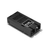
HFCT5201B Avago Technologies US Inc., HFCT5201B Datasheet - Page 7

HFCT5201B
Manufacturer Part Number
HFCT5201B
Description
Manufacturer
Avago Technologies US Inc.
Datasheet
1.HFCT5201B.pdf
(8 pages)
Specifications of HFCT5201B
Optical Fiber Type
TX/RX
Data Transfer Rate
155Mbps
Operating Temperature Classification
Commercial
Peak Wavelength
1360nm
Operating Supply Voltage (min)
4.75V
Operating Supply Voltage (typ)
5V
Operating Supply Voltage (max)
5.25V
Output Current
30mA
Operating Temp Range
0C to 70C
Pin Count
18
Lead Free Status / RoHS Status
Not Compliant
Table 2. Pin Out Table
7
Pin
Mounting Studs
1
2
3
4
5
6
7
8
9
10
11
12
13
14
15
16
17
18
Symbol
N/C
N/C
N/C
N/C
L
L
TX
N/C
P
V
TD+
TD‑
V
V
SD
RD‑
RD+
V
MON(‑)
MON(+)
MON
EET
CCT
CCR
EER
DIS
Functional Description
The mounting studs are provided for transceiver mechanical attachment to the circuit
board. They are embedded in the non‑conductive plastic housing and are not connected
to the transceiver internal circuit. They should be soldered into plated‑through holes on the
printed circuit board.
Laser Bias Monitor (‑)This analog current is monitored by measuring the voltage drop across
a 10 ohm resistor placed between high impedance resistors connected to pins 5 and 6 inter‑
nal to the transceiver.
Laser Bias Monitor (+)This analog current is monitored by measuring the voltage drop across
a 10 ohm resistor placed between high impedance resistors connected to pins 5 and 6 inter‑
nal to the transceiver.
Transmitter DisableTransmitter Output Disabled: V
Uncertain: V
open circuit
Power MonitorThe analog voltage measured at this high impedance output provides an
indication of whether the optical power output of the Laser Diode is operating within the
normal specified power output range per the following relationships:High Light Indication:
V
Transmitter Signal GroundDirectly connet this pin to the transmitter signal ground plane.
Transmitter Data InTerminate this high‑speed, differential Transmitter Data input with stand‑
ard PECL techniques at the tranmitter input pin.
Transmitter Data In BarTerminate this high‑speed, differential Transmitter Data input with
standard PECK techniques at the transmitter input pin.
Transmitter Power SupplyProvide +5 V dc via the recommended transmitter power supply
filter circuit.Locate the power supply filter circuit as close as possible to the V
Receiver Power SupplyProvide +5 V dc via the recommended receiver power supply filter
circuit.Locate the power supply filter circuit as close as possible to the V
Signal DetectNormal input optical levels to the receiver result in a logic “1” output.Low input
optical levels to the receiver result in a fault indication shown by a logic “0” output.Signal
Detect is a single‑ended, low‑power, PECL output. For low power applications a 10kW ter‑
mination resistor may be connected to V
output can be used to drive a PECL input on an upstream circuit, such as, Signal Detect input
and Loss of Signal‑bar input.
Receiver Data Out BarTerminte this high‑speed, differental, PECL output with standard PECL
techniques at the follow‑on device input pin.
Receiver Data OutTerminate this high‑speed, differential, PECL output with standard PECL
techniques at the follow‑on device input pin.
Receiver Signal GroundDirectly connect this pin to receiver signal ground plane.
9
> V
EET
+1.7 VNormal Operation: V
CCT
‑4.2 V < V
7
< V
CCT
‑1.5 VTransmitter Output Enabled: V
9
~= V
EE
EET
to achieve PECL output levels.This Signal Detect
+1.2 VLow Light Indication: V
CCT
‑1.5V < V
7
< V
CCT
EET
Transmitter Output
CCR
< V
9
pin.
7
< V
CCT
< V
EET
pin.
CCT
+0.7 V
‑4.2 V or


