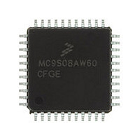
MC9S08AW60CFGE Freescale, MC9S08AW60CFGE Datasheet - Page 197

MC9S08AW60CFGE
Manufacturer Part Number
MC9S08AW60CFGE
Description
Manufacturer
Freescale
Datasheet
1.MC9S08AW60CFGE.pdf
(336 pages)
Specifications of MC9S08AW60CFGE
Cpu Family
HCS08
Device Core Size
8b
Frequency (max)
40MHz
Interface Type
I2C/SCI/SPI
Total Internal Ram Size
2KB
# I/os (max)
34
Number Of Timers - General Purpose
8
Operating Supply Voltage (typ)
3.3/5V
Operating Supply Voltage (max)
5.5V
Operating Supply Voltage (min)
2.7V
On-chip Adc
8-chx10-bit
Instruction Set Architecture
CISC
Operating Temp Range
-40C to 85C
Operating Temperature Classification
Industrial
Mounting
Surface Mount
Pin Count
44
Package Type
LQFP
Program Memory Type
Flash
Program Memory Size
60KB
Lead Free Status / RoHS Status
Compliant
Available stocks
Company
Part Number
Manufacturer
Quantity
Price
Company:
Part Number:
MC9S08AW60CFGE
Manufacturer:
Freescale Semiconductor
Quantity:
10 000
Company:
Part Number:
MC9S08AW60CFGER
Manufacturer:
Freescale Semiconductor
Quantity:
10 000
- Current page: 197 of 336
- Download datasheet (7Mb)
11.2.4
This register has eight read-only status flags. Writes have no effect. Special software sequences (which do
not involve writing to this register) are used to clear these status flags.
Freescale Semiconductor
Reset
Field
RWU
SBK
RE
2
1
0
W
R
TDRE
SCI Status Register 1 (SCIxS1)
Receiver Enable — When the SCI receiver is off, the RxD pin reverts to being a general-purpose port I/O pin. If
LOOPS = 1 the RxD pin reverts to being a general-purpose I/O pin even if RE = 1.
0 Receiver off.
1 Receiver on.
Receiver Wakeup Control — This bit can be written to 1 to place the SCI receiver in a standby state where it
waits for automatic hardware detection of a selected wakeup condition. The wakeup condition is either an idle
line between messages (WAKE = 0, idle-line wakeup), or a logic 1 in the most significant data bit in a character
(WAKE = 1, address-mark wakeup). Application software sets RWU and (normally) a selected hardware
condition automatically clears RWU. Refer to
0 Normal SCI receiver operation.
1 SCI receiver in standby waiting for wakeup condition.
Send Break — Writing a 1 and then a 0 to SBK queues a break character in the transmit data stream. Additional
break characters of 10 or 11 (13 or 14 if BRK13 = 1) bit times of logic 0 are queued as long as SBK = 1.
Depending on the timing of the set and clear of SBK relative to the information currently being transmitted, a
second break character may be queued before software clears SBK. Refer to
Queued
0 Normal transmitter operation.
1 Queue break character(s) to be sent.
1
7
Idle” for more details.
= Unimplemented or Reserved
TC
1
6
Table 11-4. SCIxC2 Field Descriptions (continued)
Figure 11-8. SCI Status Register 1 (SCIxS1)
MC9S08AC16 Series Data Sheet, Rev. 8
RDRF
0
5
IDLE
Section 11.3.3.2, “Receiver Wakeup
0
4
Description
OR
3
0
Serial Communications Interface (S08SCIV4)
NF
0
2
Section 11.3.2.1, “Send Break and
Operation” for more details.
FE
0
1
PF
0
0
197
Related parts for MC9S08AW60CFGE
Image
Part Number
Description
Manufacturer
Datasheet
Request
R

Part Number:
Description:
TOWER ELEVATOR BOARDS HARDWARE
Manufacturer:
Freescale Semiconductor
Datasheet:

Part Number:
Description:
TOWER SERIAL I/O HARDWARE
Manufacturer:
Freescale Semiconductor
Datasheet:

Part Number:
Description:
LCD MODULE FOR TWR SYSTEM
Manufacturer:
Freescale Semiconductor
Datasheet:

Part Number:
Description:
DAUGHTER LCD WVGA I.MX51
Manufacturer:
Freescale Semiconductor
Datasheet:

Part Number:
Description:
TOWER SYSTEM BOARD MPC5125
Manufacturer:
Freescale Semiconductor
Datasheet:

Part Number:
Description:
KIT EVALUATION I.MX51
Manufacturer:
Freescale Semiconductor
Datasheet:

Part Number:
Description:
KIT DEVELOPMENT WINCE IMX25
Manufacturer:
Freescale Semiconductor
Datasheet:

Part Number:
Description:
TOWER SYSTEM KIT MPC5125
Manufacturer:
Freescale Semiconductor
Datasheet:

Part Number:
Description:
TOWER SYSTEM BOARD K40X256
Manufacturer:
Freescale Semiconductor
Datasheet:

Part Number:
Description:
TOWER SYSTEM KIT K40X256
Manufacturer:
Freescale Semiconductor
Datasheet:

Part Number:
Description:
Microcontrollers (MCU) MX28 PLATFORM DEV KIT
Manufacturer:
Freescale Semiconductor
Datasheet:

Part Number:
Description:
MCU, MPU & DSP Development Tools IAR KickStart Kit for Kinetis K60
Manufacturer:
Freescale Semiconductor
Datasheet:

Part Number:
Description:
24BIT HDMI MX535/08
Manufacturer:
Freescale Semiconductor
Datasheet:
Part Number:
Description:
Manufacturer:
Freescale Semiconductor, Inc
Datasheet:
Part Number:
Description:
Manufacturer:
Freescale Semiconductor, Inc
Datasheet:


