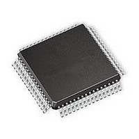
PIC16F1526-I/PT Microchip Technology, PIC16F1526-I/PT Datasheet - Page 184

PIC16F1526-I/PT
Manufacturer Part Number
PIC16F1526-I/PT
Description
MCU 14KB FLASH 768B RAM 64-TQFP
Manufacturer
Microchip Technology
Datasheet
1.PIC16F1526-IPT.pdf
(354 pages)
Specifications of PIC16F1526-I/PT
Processor Series
PIC16F
Core
PIC
Program Memory Type
Flash
Program Memory Size
14 KB
Data Ram Size
768 B
Interface Type
MI2C, SPI, EUSART
Number Of Timers
9
Operating Supply Voltage
1.8 V to 5.5 V
Maximum Operating Temperature
+ 85 C
Mounting Style
SMD/SMT
Package / Case
TQFP-64
Development Tools By Supplier
MPLAB IDE Software
Minimum Operating Temperature
- 40 C
Lead Free Status / Rohs Status
Lead free / RoHS Compliant
Available stocks
Company
Part Number
Manufacturer
Quantity
Price
Company:
Part Number:
PIC16F1526-I/PT
Manufacturer:
Microchip Technology
Quantity:
10 000
Part Number:
PIC16F1526-I/PT
Manufacturer:
MICROCHIP/微芯
Quantity:
20 000
- Current page: 184 of 354
- Download datasheet (3Mb)
PIC16(L)F1526/27
20.1
The Capture mode function described in this section is
available and identical for CCP modules.
Capture mode makes use of the 16-bit Timer1/3/5
resource. When an event occurs on the CCPx pin, the
16-bit CCPRxH:CCPRxL register pair captures and
stores the 16-bit value of the TMRxH:TMRxL register
pair, respectively. An event is defined as one of the
following and is configured by the CCPxM<3:0> bits of
the CCPxCON register:
• Every falling edge
• Every rising edge
• Every 4th rising edge
• Every 16th rising edge
When a capture is made, the Interrupt Request flag bit
CCPxIF of the PIRx register is set. The interrupt flag
must be cleared in software. If another capture occurs
before the value in the CCPRxH, CCPRxL register pair
is read, the old captured value is overwritten by the new
captured value.
Figure 20-1
operation.
20.1.1
In Capture mode, the CCPx pin should be configured
as an input by setting the associated TRIS control bit.
Also, the CCP2x pin function can be moved to
alternative pins using the APFCON register. Refer to
Section 12.1 “Alternate Pin Function”
details.
FIGURE 20-1:
DS41458A-page 184
CCPx
Pin
Note:
System Clock (F
Capture Mode
Edge Detect
CCP PIN CONFIGURATION
If the CCPx pin is configured as an output,
a write to the port can cause a capture
condition.
Prescaler
1, 4, 16
shows a simplified diagram of the Capture
and
CCPxM<3:0>
OSC
)
Set Flag bit CCPxIF
(PIRx register)
CAPTURE MODE
OPERATION BLOCK
DIAGRAM
Capture
Enable
CCPRxH
TMRxH
CCPRxL
for more
TMRxL
Preliminary
20.1.2
Timer1/3/5 must be running in Timer mode or
Synchronized Counter mode for the CCP module to use
the capture feature. In Asynchronous Counter mode, the
capture operation may not work.
See
Control”
Timer1/3/5.
TABLE 20-1:
20.1.3
When the Capture mode is changed, a false capture
interrupt may be generated. The user should keep the
CCPxIE interrupt enable bit of the PIEx register clear to
avoid false interrupts. Additionally, the user should
clear the CCPxIF interrupt flag bit of the PIRx register
following any change in Operating mode.
Note:
CCP10
Section 18.0 “Timer1/3/5 Module with Gate
CCP1
CCP2
CCP3
CCP4
CCP5
CCP6
CCP7
CCP8
CCP9
CCP
for
TIMER1/3/5 MODE RESOURCE
SOFTWARE INTERRUPT MODE
Clocking Timer1/3/5 from the system clock
(F
mode. In order for Capture mode to
recognize the trigger event on the CCPx
pin, Timer1/3/5 must be clocked from the
instruction clock (F
external clock source.
OSC
more
) should not be used in Capture
CCPx CAPTURE TIMER1/3/5
RESOURCES
TMR1
●
●
●
●
●
●
●
●
●
●
2011 Microchip Technology Inc.
information
OSC
TMR3
●
●
●
●
●
/4) or from an
on
configuring
TMR5
●
●
●
●
●
Related parts for PIC16F1526-I/PT
Image
Part Number
Description
Manufacturer
Datasheet
Request
R

Part Number:
Description:
IC, 8BIT MCU, PIC16F, 32MHZ, SOIC-18
Manufacturer:
Microchip Technology
Datasheet:

Part Number:
Description:
IC, 8BIT MCU, PIC16F, 32MHZ, SSOP-20
Manufacturer:
Microchip Technology
Datasheet:

Part Number:
Description:
IC, 8BIT MCU, PIC16F, 32MHZ, DIP-18
Manufacturer:
Microchip Technology
Datasheet:

Part Number:
Description:
IC, 8BIT MCU, PIC16F, 32MHZ, QFN-28
Manufacturer:
Microchip Technology
Datasheet:

Part Number:
Description:
IC, 8BIT MCU, PIC16F, 32MHZ, QFN-28
Manufacturer:
Microchip Technology
Datasheet:

Part Number:
Description:
IC, 8BIT MCU, PIC16F, 32MHZ, QFN-28
Manufacturer:
Microchip Technology
Datasheet:

Part Number:
Description:
IC, 8BIT MCU, PIC16F, 32MHZ, SSOP-20
Manufacturer:
Microchip Technology
Datasheet:

Part Number:
Description:
IC, 8BIT MCU, PIC16F, 20MHZ, DIP-40
Manufacturer:
Microchip Technology
Datasheet:

Part Number:
Description:
IC, 8BIT MCU, PIC16F, 32MHZ, QFN-28
Manufacturer:
Microchip Technology
Datasheet:

Part Number:
Description:
IC, 8BIT MCU, PIC16F, 20MHZ, MQFP-44
Manufacturer:
Microchip Technology
Datasheet:

Part Number:
Description:
IC, 8BIT MCU, PIC16F, 20MHZ, QFN-20
Manufacturer:
Microchip Technology
Datasheet:

Part Number:
Description:
IC, 8BIT MCU, PIC16F, 32MHZ, QFN-28
Manufacturer:
Microchip Technology
Datasheet:

Part Number:
Description:
7 KB Flash, 384 Bytes RAM, 32 MHz Int. Osc, 16 I/0, Enhanced Mid Range Core, Low
Manufacturer:
Microchip Technology

Part Number:
Description:
14KB Flash, 512B RAM, 256B EEPROM, LCD, 1.8-5.5V 40 UQFN 5x5x0.5mm TUBE
Manufacturer:
Microchip Technology
Datasheet:

Part Number:
Description:
14KB Flash, 512B RAM, 256B EEPROM, LCD, 1.8-5.5V 40 UQFN 5x5x0.5mm TUBE
Manufacturer:
Microchip Technology


