PIC16F1526-I/PT Microchip Technology, PIC16F1526-I/PT Datasheet - Page 249
PIC16F1526-I/PT
Manufacturer Part Number
PIC16F1526-I/PT
Description
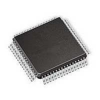
MCU 14KB FLASH 768B RAM 64-TQFP
Manufacturer
Microchip Technology
Datasheet
1.PIC16F1526-IPT.pdf
(354 pages)
Specifications of PIC16F1526-I/PT
Processor Series
PIC16F
Core
PIC
Program Memory Type
Flash
Program Memory Size
14 KB
Data Ram Size
768 B
Interface Type
MI2C, SPI, EUSART
Number Of Timers
9
Operating Supply Voltage
1.8 V to 5.5 V
Maximum Operating Temperature
+ 85 C
Mounting Style
SMD/SMT
Package / Case
TQFP-64
Development Tools By Supplier
MPLAB IDE Software
Minimum Operating Temperature
- 40 C
Lead Free Status / Rohs Status
Lead free / RoHS Compliant
Available stocks
Company
Part Number
Manufacturer
Quantity
Price
Company:

Part Number:
PIC16F1526-I/PT
Manufacturer:
Microchip Technology
Quantity:
10 000
Part Number:
PIC16F1526-I/PT
Manufacturer:
MICROCHIP/微芯
Quantity:
20 000


21.8
REGISTER 21-1:
2011 Microchip Technology Inc.
bit 7
Legend:
R = Readable bit
u = Bit is unchanged
‘1’ = Bit is set
bit 7
bit 6
bit 5
bit 4
bit 3
bit 2
bit 1
R/W-0/0
SMP
MSSP Control Registers
SMP: SPI Data Input Sample bit
SPI Master mode:
1 = Input data sampled at end of data output time
0 = Input data sampled at middle of data output time
SPI Slave mode:
SMP must be cleared when SPI is used in Slave mode
In I
1 = Slew rate control disabled for standard speed mode (100 kHz and 1 MHz)
0 = Slew rate control enabled for high speed mode (400 kHz)
CKE: SPI Clock Edge Select bit (SPI mode only)
In SPI Master or Slave mode:
1 = Transmit occurs on transition from active to Idle clock state
0 = Transmit occurs on transition from Idle to active clock state
In I
1 = Enable input logic so that thresholds are compliant with SMBus specification
0 = Disable SMBus specific inputs
D/A: Data/Address bit (I
1 = Indicates that the last byte received or transmitted was data
0 = Indicates that the last byte received or transmitted was address
P: Stop bit
(I
1 = Indicates that a Stop bit has been detected last (this bit is ‘ 0 ’ on Reset)
0 = Stop bit was not detected last
S: Start bit
(I
1 = Indicates that a Start bit has been detected last (this bit is ‘ 0 ’ on Reset)
0 = Start bit was not detected last
R/W: Read/Write bit information (I
This bit holds the R/W bit information following the last address match. This bit is only valid from the address match
to the next Start bit, Stop bit, or not ACK bit.
In I
1 = Read
0 = Write
In I
1 = Transmit is in progress
0 = Transmit is not in progress
UA: Update Address bit (10-bit I
1 = Indicates that the user needs to update the address in the SSPxADD register
0 = Address does not need to be updated
2
2
C mode only. This bit is cleared when the MSSPx module is disabled, SSPxEN is cleared.)
C mode only. This bit is cleared when the MSSPx module is disabled, SSPxEN is cleared.)
2
2
2
2
R/W-0/0
C Master or Slave mode:
C™ mode only:
C Slave mode:
C Master mode:
CKE
OR-ing this bit with SEN, RSEN, PEN, RCEN or ACKEN will indicate if the MSSPx is in Idle mode.
SSPxSTAT: SSPx STATUS REGISTER
W = Writable bit
x = Bit is unknown
‘0’ = Bit is cleared
R-0/0
D/A
2
C mode only)
2
C mode only)
2
C mode only)
R-0/0
Preliminary
P
U = Unimplemented bit, read as ‘0’
-n/n = Value at POR and BOR/Value at all other Resets
R-0/0
S
PIC16(L)F1526/27
R-0/0
R/W
R-0/0
UA
DS41458A-page 249
R-0/0
BF
bit 0
Related parts for PIC16F1526-I/PT
Image
Part Number
Description
Manufacturer
Datasheet
Request
R

Part Number:
Description:
IC, 8BIT MCU, PIC16F, 32MHZ, SOIC-18
Manufacturer:
Microchip Technology
Datasheet:

Part Number:
Description:
IC, 8BIT MCU, PIC16F, 32MHZ, SSOP-20
Manufacturer:
Microchip Technology
Datasheet:

Part Number:
Description:
IC, 8BIT MCU, PIC16F, 32MHZ, DIP-18
Manufacturer:
Microchip Technology
Datasheet:

Part Number:
Description:
IC, 8BIT MCU, PIC16F, 32MHZ, QFN-28
Manufacturer:
Microchip Technology
Datasheet:

Part Number:
Description:
IC, 8BIT MCU, PIC16F, 32MHZ, QFN-28
Manufacturer:
Microchip Technology
Datasheet:
Part Number:
Description:
IC, 8BIT MCU, PIC16F, 32MHZ, QFN-28
Manufacturer:
Microchip Technology
Datasheet:
Part Number:
Description:
IC, 8BIT MCU, PIC16F, 32MHZ, SSOP-20
Manufacturer:
Microchip Technology
Datasheet:

Part Number:
Description:
IC, 8BIT MCU, PIC16F, 20MHZ, DIP-40
Manufacturer:
Microchip Technology
Datasheet:

Part Number:
Description:
IC, 8BIT MCU, PIC16F, 32MHZ, QFN-28
Manufacturer:
Microchip Technology
Datasheet:

Part Number:
Description:
IC, 8BIT MCU, PIC16F, 20MHZ, MQFP-44
Manufacturer:
Microchip Technology
Datasheet:

Part Number:
Description:
IC, 8BIT MCU, PIC16F, 20MHZ, QFN-20
Manufacturer:
Microchip Technology
Datasheet:
Part Number:
Description:
IC, 8BIT MCU, PIC16F, 32MHZ, QFN-28
Manufacturer:
Microchip Technology
Datasheet:
Part Number:
Description:
7 KB Flash, 384 Bytes RAM, 32 MHz Int. Osc, 16 I/0, Enhanced Mid Range Core, Low
Manufacturer:
Microchip Technology

Part Number:
Description:
14KB Flash, 512B RAM, 256B EEPROM, LCD, 1.8-5.5V 40 UQFN 5x5x0.5mm TUBE
Manufacturer:
Microchip Technology
Datasheet:
Part Number:
Description:
14KB Flash, 512B RAM, 256B EEPROM, LCD, 1.8-5.5V 40 UQFN 5x5x0.5mm TUBE
Manufacturer:
Microchip Technology