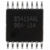
ICS854104AGLF IDT, Integrated Device Technology Inc, ICS854104AGLF Datasheet - Page 4

ICS854104AGLF
Manufacturer Part Number
ICS854104AGLF
Description
IC FANOUT BUFF DIFF-LVDS 16TSSOP
Manufacturer
IDT, Integrated Device Technology Inc
Series
HiPerClockS™r
Type
Fanout Buffer (Distribution)r
Datasheet
1.ICS854104AGLF.pdf
(15 pages)
Specifications of ICS854104AGLF
Number Of Circuits
1
Ratio - Input:output
1:4
Differential - Input:output
Yes/Yes
Input
HCSL, LVDS, LVHSTL, LVPECL, SSTL
Output
LVDS
Frequency - Max
700MHz
Voltage - Supply
3.135 V ~ 3.465 V
Operating Temperature
0°C ~ 70°C
Mounting Type
Surface Mount
Package / Case
16-TSSOP
Frequency-max
700MHz
Lead Free Status / RoHS Status
Lead free / RoHS Compliant
Other names
800-1183
800-1183-5
800-1183
854104AGLF
800-1183-5
800-1183
854104AGLF
Available stocks
Company
Part Number
Manufacturer
Quantity
Price
Company:
Part Number:
ICS854104AGLF
Manufacturer:
Microchip
Quantity:
343
ICS854104 Data Sheet
Table 4D. LVDS DC Characteristics, V
Table 5. AC Characteristics, V
NOTE: Electrical parameters are guaranteed over the specified ambient operating temperature range, which is established when the device is
mounted in a test socket with maintained transverse airflow greater than 500 lfpm. The device will meet specifications after thermal equilibrium
has been reached under these conditions.
NOTE: All parameters measured at f
NOTE 1: Measured from the differential input crossing point to the differential output crossing point.
NOTE 2: Defined as skew between outputs at the same supply voltage and with equal load conditions. Measured at the differential crossing
point of the input to the differential output crossing point.
NOTE 3: Defined as skew between outputs on different devices operating at the same supply voltages and with equal load conditions. Using
the same type of inputs on each device, the outputs are measured at the differential cross points.
NOTE 4: This parameter is defined in accordance with JEDEC Standard 65.
ICS854104AG REVISION A AUGUST 14, 2009
Symbol
V
∆V
V
∆V
Symbol
f
t
tjit
tsk(o)
tsk(pp)
t
odc
MAX
PD
R
OD
OS
/ t
OD
OS
F
Parameter
Output Frequency
Propagation Delay; NOTE 1
Buffer Additive Phase Jitter, RMS;
refer to Additive Phase Jitter
Section
Output Skew; NOTE 2, 4
Part-to-Part Skew; NOTE 3, 4
Output Rise/Fall Time
Output Duty Cycle
Parameter
Differential Output Voltage
V
Offset Voltage
V
OD
OS
Magnitude Change
Magnitude Change
DD
MAX
= 3.3V ± 5%, T
unless noted otherwise.
DD
= 3.3V ± 5%, T
Integration Range: 12kHz – 20MHz)
A
Test Conditions
= 0°C to 70°C
Test Conditions
155.52MHz,
20% to 80%
A
= 0°C to 70°C
4
Minimum
LOW SKEW, 1-TO-4, DIFFERENTIAL-TO-LVDS FANOUT BUFFER
250
1.2
Minimum
180
0.9
45
Typical
350
1.3
Typical
0.232
©2009 Integrated Device Technology, Inc.
Maximum
Maximum
1.45
450
50
50
700
350
660
1.3
50
55
Units
Units
mV
mV
mV
MHz
V
ps
ps
ps
ps
ns
%


