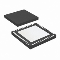
LMK03200ISQE/NOPB National Semiconductor, LMK03200ISQE/NOPB Datasheet - Page 11

LMK03200ISQE/NOPB
Manufacturer Part Number
LMK03200ISQE/NOPB
Description
IC CLOCK CONDITIONER PREC 48-LLP
Manufacturer
National Semiconductor
Type
Clock Conditionerr
Datasheet
1.LMK03200ISQENOPB.pdf
(40 pages)
Specifications of LMK03200ISQE/NOPB
Pll
Yes
Input
Clock
Output
LVDS, LVPECL
Number Of Circuits
1
Ratio - Input:output
1:9
Differential - Input:output
Yes/Yes
Frequency - Max
1.296GHz
Divider/multiplier
Yes/No
Voltage - Supply
3.15 V ~ 3.45 V
Operating Temperature
-40°C ~ 85°C
Mounting Type
Surface Mount
Package / Case
48-LLP
Frequency-max
1.296GHz
Lead Free Status / RoHS Status
Lead free / RoHS Compliant
Other names
LMK03200ISQETR
Available stocks
Company
Part Number
Manufacturer
Quantity
Price
Company:
Part Number:
LMK03200ISQE/NOPB
Manufacturer:
NSC
Quantity:
72
t
t
t
t
t
t
t
CS
CH
CWH
CWL
ES
CES
EWH
Note 4: The Electrical Characteristics table lists guaranteed specifications under the listed Recommended Operating Conditions except as otherwise modified
or specified by the Electrical Characteristics Conditions and/or Notes. Typical specifications are estimations only and are not guaranteed.
Note 5: See Section
Note 6: See Section
Note 7: A specification in modeling PLL in-band phase noise is the 1/f flicker noise, L
dB/decade slope. PN10kHz is normalized to a 10 kHz offset and a 1 GHz carrier frequency. PN10kHz = L
(f) is the single side band phase noise of only the flicker noise's contribution to total noise, L(f). To measure L
slope close to the carrier. A high compare frequency and a clean crystal are important to isolating this noise source from the total phase noise, L(f). L
can be masked by the reference oscillator performance if a low power or noisy source is used. The total PLL in-band phase noise performance is the sum of
L
Note 8: A specification in modeling PLL in-band phase noise is the Normalized Phase Noise Contribution, L
L
detector frequency of the synthesizer. L
smaller then the loop bandwidth of the PLL, and yet large enough to avoid a substantial noise contribution from the reference and flicker noise. L
masked by the reference oscillator performance if a low power or noisy source is used.
Note 9: Allowable Temperature Drift for Continuous Lock is how far the temperature can drift in either direction and stay in lock from the ambient temperature
and programmed state at which the device was when the frequency calibration routine was run. The action of programming the R15 register, even to the same
value, when 0_DELAY_MODE = 0 activates a frequency calibration routine. This implies that the device will work over the entire frequency range, but if the
temperature drifts more than the maximum allowable drift for continuous lock, then it will be necessary to reprogram the R15 register while 0_DELAY_MODE =
0 to ensure that the device stays in lock. Regardless of what temperature the device was initially programmed at, the ambient temperature can never drift outside
the range of -40 °C
R15 is programmed except for 0_DELAY_MODE and PLL_N for the purpose of enabling 0-delay mode.
Note 10: The lower sensitivity indicates the typical sensitivity at the lower end of the tuning range, the higher sensitivity at the higher end of the tuning range
Note 11: Output power varies as a function of frequency. When a range is shown, the higher output power applies to the lower frequency and the lower output
power applies to the higher frequency.
Note 12: The Clock Distribution Section includes all parts of the device except the PLL and VCO sections. Typical Additive Jitter specifications apply to the clock
distribution section only and this adds in an RMS fashion to the shaped jitter of the PLL and the VCO.
Note 13: Specification is guaranteed by characterization and is not tested in production.
Note 14: Applies to GOE, LD, and SYNC*.
Note 15: Applies to CLKuWire, DATAuWire, and LEuWire.
Serial Data Timing Diagram
Data bits set on the DATAuWire signal are clocked into a shift register, MSB first, on each rising edge of the CLKuWire signal. On
the rising edge of the LEuWire signal, the data is sent from the shift register to the addressed register determined by the LSB bits.
After the programming is complete the CLKuWire, DATAuWire, and LEuWire signals should be returned to a low state. It is rec-
ommended that the slew rate of CLKuWire, DATAuWire, and LEuWire should be at least 30 V/μs.
Symbol
PLL_flicker
PLL_flat
(f) – 20log(N) – 10log(f
(f) and L
Data to Clock Set Up Time
Data to Clock Hold Time
Clock Pulse Width High
Clock Pulse Width Low
Clock to Enable Set Up Time
Enable to Clock Set Up Time
Enable Pulse Width High
PLL_flat
≤
3.5 CURRENT CONSUMPTION / POWER DISSIPATION CALCULATIONS
3.10 DIFFERENTIAL VOLTAGE MEASUREMENT TERMINOLOGY
T
(f).
A
≤
85 °C without violating specifications. For this specification to be valid, the programmed state of the device must not change after
COMP
). L
Parameter
PLL_flat
PLL_flat
(f) is the single side band phase noise measured at an offset frequency, f, in a 1 Hz Bandwidth and f
(f) contributes to the total noise, L(f). To measure L
MICROWIRE Timing
See Data Input Timing
See Data Input Timing
See Data Input Timing
See Data Input Timing
See Data Input Timing
See Data Input Timing
See Data Input Timing
11
PLL_flicker
Conditions
for more information.
(f), which is dominant close to the carrier. Flicker noise has a 10
PLL_flat
for more information.
(f) the offset frequency, f, must be chosen sufficiently
PLL_flicker
PLL_flat
PLL_flicker
(10 kHz) - 20log(Fout / 1 GHz), where L
(f), of the PLL and is defined as PN1Hz =
(f) it is important to be on the 10 dB/decade
Min
25
25
25
25
25
25
8
Typ
COMP
Max
PLL_flat
www.national.com
is the phase
30088703
PLL_flicker
(f) can be
PLL_flicker
Units
ns
ns
ns
ns
ns
ns
ns
(f)


