LMK03200ISQE/NOPB National Semiconductor, LMK03200ISQE/NOPB Datasheet - Page 26
LMK03200ISQE/NOPB
Manufacturer Part Number
LMK03200ISQE/NOPB
Description
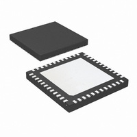
IC CLOCK CONDITIONER PREC 48-LLP
Manufacturer
National Semiconductor
Type
Clock Conditionerr
Datasheet
1.LMK03200ISQENOPB.pdf
(40 pages)
Specifications of LMK03200ISQE/NOPB
Pll
Yes
Input
Clock
Output
LVDS, LVPECL
Number Of Circuits
1
Ratio - Input:output
1:9
Differential - Input:output
Yes/Yes
Frequency - Max
1.296GHz
Divider/multiplier
Yes/No
Voltage - Supply
3.15 V ~ 3.45 V
Operating Temperature
-40°C ~ 85°C
Mounting Type
Surface Mount
Package / Case
48-LLP
Frequency-max
1.296GHz
Lead Free Status / RoHS Status
Lead free / RoHS Compliant
Other names
LMK03200ISQETR
Available stocks
Company
Part Number
Manufacturer
Quantity
Price
Company:

Part Number:
LMK03200ISQE/NOPB
Manufacturer:
NSC
Quantity:
72


www.national.com
2.4.7 CLKoutX_DIV [7:0] -- Clock Output Dividers
These bits control the clock output divider value. In order for
these dividers to be active, the respective CLKoutX_MUX bit
must be set to either "Divided" or "Divided and Delayed"
mode. After all the dividers are programed, the SYNC* pin
must be used to ensure that all edges of the clock outputs are
aligned. The Clock Output Dividers follow the VCO Divider so
the final clock divide for an output is VCO Divider × Clock
Output Divider. By adding the divider block to the output path
a fixed delay of approximately 100 ps is incurred.
The actual Clock Output Divide value is twice the binary value
programmed as listed in the table below.
2.4.8 CLKoutX_DLY [3:0] -- Clock Output Delays
These bits control the delay stages for each clock output. In
order for these delays to be active, the respective
CLKoutX_MUX bit must be set to either "Delayed" or "Divided
and Delayed" mode. By adding the delay block to the output
path a fixed delay of approximately 400 ps is incurred in ad-
dition to the delay shown in the table below.
0
0
0
0
0
0
1
.
CLKoutX_DLY [3:0]
0
0
0
0
0
0
1
.
CLKoutX_DIV [7:0]
0
0
0
0
0
0
1
.
10
11
12
13
14
15
0
1
2
3
4
5
6
7
8
9
0
0
0
0
0
0
1
.
0
0
0
0
0
0
1
.
0
0
0
0
1
1
1
.
0
0
1
1
0
0
1
.
Delay (ps)
0 (default)
0
1
0
1
0
1
1
.
1050
1200
1350
1500
1650
1800
1950
2100
2250
150
300
450
600
750
900
Clock Output
Divider value
2 (default)
Invalid
510
10
...
4
6
8
26
2.4.9 CLKoutX_EN bit -- Clock Output Enables
These bits control whether an individual clock output is en-
abled or not. If the EN_CLKout_Global bit is set to zero or if
GOE pin is held low, all CLKoutX_EN bit states will be ignored
and all clock outputs will be disabled.
2.5 Register R8
There are no user programmable bits in register R8. Register
R8 is programmed as shown in the section for optimum phase
noise performance.
2.6 Register R9
The programming of register R9 is optional. If it is not pro-
grammed the bit Vboost will be defaulted to 0, which is the
test condition for all electrical characteristics.
2.6.1 Vboost bit -- Voltage Boost
By enabling this bit, the voltage output levels for all clock out-
puts is increased. Also, the noise floor is improved
CLKoutX_EN
Vboost
bit
0
1
0
1
EN_CLKout_Global bit = 1
GOE pin = High / No
Voltage Output
Typical LVDS
Conditions
Connect
(mV)
350
390
Typical LVPECL
Voltage Output
CLKoutX
Disabled
(mV)
(default)
Enabled
810
865
State
Related parts for LMK03200ISQE/NOPB
Image
Part Number
Description
Manufacturer
Datasheet
Request
R

Part Number:
Description:
National Semiconductor [8-Bit D/A Converter]
Manufacturer:
National Semiconductor
Datasheet:
Part Number:
Description:
National Semiconductor [Media Coprocessor]
Manufacturer:
National Semiconductor
Datasheet:
Part Number:
Description:
Digitally Controlled Tone and Volume Circuit with Stereo Audio Power Amplifier, Microphone Preamp Stage and National 3D Sound
Manufacturer:
National Semiconductor
Datasheet:
Part Number:
Description:
Digitally Controlled Tone and Volume Circuit with Stereo Audio Power Amplifier, Microphone Preamp Stage and National 3D Sound
Manufacturer:
National Semiconductor
Datasheet:
Part Number:
Description:
AC97 Rev 2 Codec with Sample Rate Conversion and National 3D Sound
Manufacturer:
National Semiconductor
Part Number:
Description:
Manufacturer:
National Semiconductor
Datasheet:
Part Number:
Description:
Manufacturer:
National Semiconductor
Datasheet:
Part Number:
Description:
General Purpose, Low Voltage, Low Power, Rail-to-Rail Output Operational Amplifiers
Manufacturer:
National Semiconductor
Datasheet:
Part Number:
Description:
8-bit 20 MSPS flash A/D converter.
Manufacturer:
National Semiconductor
Datasheet:
Part Number:
Description:
Low Noise Quad Operational Amplifier
Manufacturer:
National Semiconductor
Datasheet:
Part Number:
Description:
Quad Differential Line Receivers
Manufacturer:
National Semiconductor
Datasheet:
Part Number:
Description:
Quad High Speed Trapezoidal? Bus Transceiver
Manufacturer:
National Semiconductor
Datasheet:
Part Number:
Description:
Dual Line Receiver
Manufacturer:
National Semiconductor
Datasheet:
Part Number:
Description:
TTL to 10k ECL Level Translator with Latch
Manufacturer:
National Semiconductor
Datasheet: