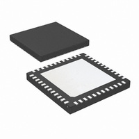
LMK03200ISQE/NOPB National Semiconductor, LMK03200ISQE/NOPB Datasheet - Page 15

LMK03200ISQE/NOPB
Manufacturer Part Number
LMK03200ISQE/NOPB
Description
IC CLOCK CONDITIONER PREC 48-LLP
Manufacturer
National Semiconductor
Type
Clock Conditionerr
Datasheet
1.LMK03200ISQENOPB.pdf
(40 pages)
Specifications of LMK03200ISQE/NOPB
Pll
Yes
Input
Clock
Output
LVDS, LVPECL
Number Of Circuits
1
Ratio - Input:output
1:9
Differential - Input:output
Yes/Yes
Frequency - Max
1.296GHz
Divider/multiplier
Yes/No
Voltage - Supply
3.15 V ~ 3.45 V
Operating Temperature
-40°C ~ 85°C
Mounting Type
Surface Mount
Package / Case
48-LLP
Frequency-max
1.296GHz
Lead Free Status / RoHS Status
Lead free / RoHS Compliant
Other names
LMK03200ISQETR
Available stocks
Company
Part Number
Manufacturer
Quantity
Price
Company:
Part Number:
LMK03200ISQE/NOPB
Manufacturer:
NSC
Quantity:
72
1.6 GLOBAL CLOCK OUTPUT SYNCHRONIZATION
The SYNC* pin synchronizes the clock outputs. SYNC* is not
used in VCO bypass mode. When the SYNC* pin is held in a
logic low state, the divided outputs are also held in a logic low
state. The bypassed outputs will continue to operate normally.
Shortly after the SYNC* pin goes high, the divided clock out-
puts are activated and will all transition to a high state simul-
taneously. All the outputs, divided and bypassed, will now be
synchronized. Clocks in the bypassed state are not affected
by SYNC* and are always synchronized with the divided out-
puts.
The SYNC* pin must be held low for greater than one clock
cycle of the output of the VCO divider, also known as the dis-
tribution path. Once this low event has been registered, the
outputs will not reflect the low state for four more cycles. This
means that the outputs will be low on the fifth rising edge of
the distribution path. Similarly once the SYNC* pin becomes
high, the outputs will not simultaneously transition high until
four more distribution path clock cycles have passed, which
is the fifth rising edge of the distribution path. See the timing
diagram in
grammed as CLKout0_MUX = Bypassed, CLKout1_MUX =
Divided, CLKout1_DIV = 2, CLKout2_MUX = Divided, and
CLKout2_DIV = 4. To synchronize the outputs, after the low
SYNC* event has been registered, it is not required to wait for
the outputs to go low before SYNC* is set high.
The SYNC* pin provides an internal pull-up resistor as shown
on the functional block diagram. If the SYNC* pin is not ter-
minated externally the clock outputs will operate normally. If
Figure 2
FIGURE 2. SYNC* Timing Diagram
for further detail. The clocks are pro-
30088704
15
the SYNC* function is not used, clock output synchronization
is not guaranteed. To ensure 0-delay to reference see section
2.2 Recommended Programing Sequence, with 0-Delay
Mode.
1.7 CLKout OUTPUT STATES
Each clock output may be individually enabled with the
CLKoutX_EN bits. Each individual output enable control bit is
gated with the Global Output Enable input pin (GOE) and the
Global Output Enable bit (EN_CLKout_Global).
All clock outputs can be disabled simultaneously if the GOE
pin is pulled low by an external signal or EN_CLKout_Global
is set to 0.
When an LVDS output is in the Off state, the outputs are at a
voltage of approximately 1.5 volts. When an LVPECL output
is in the Off state, the outputs are at a voltage of approximately
1 volt.
1.8 GLOBAL OUTPUT ENABLE AND LOCK DETECT
The GOE pin provides an internal pull-up resistor as shown
on the functional block diagram. If it is not terminated exter-
nally, the clock output states are determined by the Clock
Output
EN_CLKout_Global bit.
By programming the PLL_MUX register to Digital Lock Detect
Active High, the Lock Detect (LD) pin can be connected to the
GOE pin in which case all outputs are set low automatically if
the synthesizer is not locked.
1.9 POWER ON RESET
When supply voltage to the device increases monotonically
from ground to Vcc, the power on reset circuit sets all registers
to their default values, see the programming section for more
information on default register values. Voltage should be ap-
plied to all Vcc pins simultaneously.
Don't care
CLKoutX
_EN bit
1
0
1
Enable
EN_CLKout
_Global bit
Don't care
1
0
1
bits
(CLKoutX_EN)
Don't care
Don't care
High / No
GOE pin
Connect
Low
Output State
CLKoutX
www.national.com
Enabled
and
Low
Off
Off
the


