LMK02000ISQ/NOPB National Semiconductor, LMK02000ISQ/NOPB Datasheet - Page 10
LMK02000ISQ/NOPB
Manufacturer Part Number
LMK02000ISQ/NOPB
Description
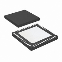
IC CLOCK CONDITIONER PREC 48-LLP
Manufacturer
National Semiconductor
Type
Clock Conditionerr
Datasheet
1.LMK02000ISQNOPB.pdf
(20 pages)
Specifications of LMK02000ISQ/NOPB
Pll
Yes
Input
Clock
Output
LVDS, LVPECL
Number Of Circuits
1
Ratio - Input:output
2:8
Differential - Input:output
Yes/Yes
Frequency - Max
800MHz
Divider/multiplier
Yes/No
Voltage - Supply
3.15 V ~ 3.45 V
Operating Temperature
-40°C ~ 85°C
Mounting Type
Surface Mount
Package / Case
48-LLP
Frequency-max
800MHz
For Use With
LMK02000EVAL-1 - BOARD EVAL WITH 245.76 VCXOLMK02000EVAL2 - BOARD EVALUATION FOR LMK02000
Lead Free Status / RoHS Status
Lead free / RoHS Compliant
Other names
LMK02000ISQ
LMK02000ISQTR
LMK02000ISQTR
Available stocks
Company
Part Number
Manufacturer
Quantity
Price
Company:

Part Number:
LMK02000ISQ/NOPB
Manufacturer:
Intersil
Quantity:
106


www.national.com
2.0 General Programming
Information
The LMK02000 device is programmed using several 32-bit
registers which control the device's operation. The registers
consist of a data field and an address field. The last 4 register
bits, ADDR[3:0] form the address field. The remaining 28 bits
form the data field DATA[27:0].
During programming, LEuWire is low and serial data is
clocked in on the rising edge of clock (MSB first). When
LEuWire goes high, data is transferred to the register bank
selected by the address field. Only registers R0 to R7, R11,
R14, and R15 need to be programmed for proper device op-
eration.
It is required to program register R14.
2.1 RECOMMENDED PROGRAMMING SEQUENCE
The recommended programming sequence involves pro-
gramming R0 with the reset bit set (RESET = 1) to ensure the
device is in a default state. It is not necessary to program R0
again, but if R0 is programmed again, the reset bit is pro-
grammed clear (RESET = 0). Registers are programmed in
order with R15 being the last register programmed. An ex-
ample programming sequence is shown below.
•
•
•
•
•
Program R0 with the reset bit set (RESET = 1). This
ensures the device is in a default state. When the reset bit
is set in R0, the other R0 bits are ignored.
— If R0 is programmed again, the reset bit is programmed
Program R0 to R7 as necessary with desired clocks with
appropriate enable, mux, divider, and delay settings.
Program R11 with DIV4 setting if necessary.
Program R14 with global clock output bit, power down
setting, PLL mux setting, and PLL R divider. It is required
to program register R14.
— R14 must be programmed in accordance with the
Program R15 with PLL charge pump gain, and PLL N
divider.
clear (RESET = 0).
register map as shown in the register map (see 2.2).
10
Related parts for LMK02000ISQ/NOPB
Image
Part Number
Description
Manufacturer
Datasheet
Request
R

Part Number:
Description:
National Semiconductor [8-Bit D/A Converter]
Manufacturer:
National Semiconductor
Datasheet:
Part Number:
Description:
National Semiconductor [Media Coprocessor]
Manufacturer:
National Semiconductor
Datasheet:
Part Number:
Description:
Digitally Controlled Tone and Volume Circuit with Stereo Audio Power Amplifier, Microphone Preamp Stage and National 3D Sound
Manufacturer:
National Semiconductor
Datasheet:
Part Number:
Description:
Digitally Controlled Tone and Volume Circuit with Stereo Audio Power Amplifier, Microphone Preamp Stage and National 3D Sound
Manufacturer:
National Semiconductor
Datasheet:
Part Number:
Description:
AC97 Rev 2 Codec with Sample Rate Conversion and National 3D Sound
Manufacturer:
National Semiconductor
Part Number:
Description:
Manufacturer:
National Semiconductor
Datasheet:
Part Number:
Description:
Manufacturer:
National Semiconductor
Datasheet:
Part Number:
Description:
General Purpose, Low Voltage, Low Power, Rail-to-Rail Output Operational Amplifiers
Manufacturer:
National Semiconductor
Datasheet:
Part Number:
Description:
8-bit 20 MSPS flash A/D converter.
Manufacturer:
National Semiconductor
Datasheet:
Part Number:
Description:
Low Noise Quad Operational Amplifier
Manufacturer:
National Semiconductor
Datasheet:
Part Number:
Description:
Quad Differential Line Receivers
Manufacturer:
National Semiconductor
Datasheet:
Part Number:
Description:
Quad High Speed Trapezoidal? Bus Transceiver
Manufacturer:
National Semiconductor
Datasheet:
Part Number:
Description:
Dual Line Receiver
Manufacturer:
National Semiconductor
Datasheet:
Part Number:
Description:
TTL to 10k ECL Level Translator with Latch
Manufacturer:
National Semiconductor
Datasheet: