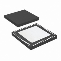
LMK02000ISQ/NOPB National Semiconductor, LMK02000ISQ/NOPB Datasheet - Page 14

LMK02000ISQ/NOPB
Manufacturer Part Number
LMK02000ISQ/NOPB
Description
IC CLOCK CONDITIONER PREC 48-LLP
Manufacturer
National Semiconductor
Type
Clock Conditionerr
Datasheet
1.LMK02000ISQNOPB.pdf
(20 pages)
Specifications of LMK02000ISQ/NOPB
Pll
Yes
Input
Clock
Output
LVDS, LVPECL
Number Of Circuits
1
Ratio - Input:output
2:8
Differential - Input:output
Yes/Yes
Frequency - Max
800MHz
Divider/multiplier
Yes/No
Voltage - Supply
3.15 V ~ 3.45 V
Operating Temperature
-40°C ~ 85°C
Mounting Type
Surface Mount
Package / Case
48-LLP
Frequency-max
800MHz
For Use With
LMK02000EVAL-1 - BOARD EVAL WITH 245.76 VCXOLMK02000EVAL2 - BOARD EVALUATION FOR LMK02000
Lead Free Status / RoHS Status
Lead free / RoHS Compliant
Other names
LMK02000ISQ
LMK02000ISQTR
LMK02000ISQTR
Available stocks
Company
Part Number
Manufacturer
Quantity
Price
Company:
Part Number:
LMK02000ISQ/NOPB
Manufacturer:
Intersil
Quantity:
106
www.national.com
2.3.3 CLKoutX_DIV[7:0] -- Clock Output Dividers
These bits control the clock output divider value. In order for
these dividers to be active, the respective CLKoutX_MUX
(See 2.3.2) bit must be set to either "Divided" or "Divided and
Delayed" mode. After all the dividers are programed, the
SYNC* pin must be used to ensure that all edges of the clock
outputs are aligned (See 1.7). By adding the divider block to
the output path a fixed delay of approximately 100 ps is in-
curred.
The actual Clock Output Divide value is twice the binary value
programmed as listed in the table below.
2.3.4 CLKoutX_DLY[3:0] -- Clock Output Delays
These bits control the delay stages for each clock output. In
order for these delays to be active, the respective
CLKoutX_MUX (See 2.3.2) bit must be set to either "Delayed"
or "Divided and Delayed" mode. By adding the delay block to
the output path a fixed delay of approximately 400 ps is in-
curred in addition to the delay shown in the table below.
0
0
0
0
0
0
1
.
CLKoutX_DLY[3:0]
0
0
0
0
0
0
1
.
CLKoutX_DIV[7:0]
0
0
0
0
0
0
1
.
10
11
12
13
0
1
2
3
4
5
6
7
8
9
0
0
0
0
0
0
1
.
0
0
0
0
0
0
1
.
0
0
0
0
1
1
1
.
0
0
1
1
0
0
1
.
Delay (ps)
0 (default)
0
1
0
1
0
1
1
.
1050
1200
1350
1500
1650
1800
1950
150
300
450
600
750
900
Clock Output
Divider value
2 (default)
Invalid
510
10
...
4
6
8
14
2.3.5 CLKoutX_EN bit -- Clock Output Enables
These bits control whether an individual clock output is en-
abled or not. If the EN_CLKout_Global bit (See 2.5.4) is set
to zero or if GOE pin is held low, all CLKoutX_EN bit states
will be ignored and all clock outputs will be disabled. See 1.8
for more information on CLKout states.
2.4 REGISTER R11
This register only has one bit and only needs to be pro-
grammed in the case that the phase detector frequency is
greater than 20 MHz and digital lock detect is used. Other-
wise, it is automatically defaulted to the correct values.
2.4.1 DIV4
This bit divides the frequency presented to the digital lock de-
tect circuitry by 4. It is necessary to get a reliable output from
the digital lock detect output in the case of a phase detector
frequency greater than 20 MHz.
2.5 REGISTER R14
The LMK02000 requires register R14 to be programmed as
shown in the register map (see 2.2).
2.5.1 PLL_R[11:0] -- R Divider Value
These bits program the PLL R Divider and are programmed
in binary fashion.
CLKoutX_EN bit
0
0
0
0
1
.
.
CLKoutX_DLY[3:0]
0
0
0
0
1
.
.
DIV4
0
0
0
0
1
0
1
.
.
0
1
0
0
0
0
1
.
.
14
15
PLL_R[11:0]
0
0
0
0
1
.
.
GOE pin = High / No
0
0
0
0
1
EN_CLKout_Global
.
.
Digital Lock Detect Circuitry Mode
0
0
0
0
1
Conditions
.
.
Connect 1
frequency
Divided by 4; Phase detector
bit = 1
Not divided; Phase detector
0
0
0
0
1
.
.
frequency > 20 MHz
0
0
0
1
1
.
.
0
0
0
0
1
.
.
≤
0
0
1
1
1
20 MHz (default)
.
.
Delay (ps)
Disabled (default)
2100
2250
0
1
0
0
1
CLKoutX State
.
.
PLL R Divide
Enabled
10 (default)
Invalid
Value
4095
...
...
1
2


