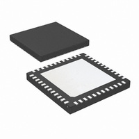
LMK02000ISQ/NOPB National Semiconductor, LMK02000ISQ/NOPB Datasheet - Page 17

LMK02000ISQ/NOPB
Manufacturer Part Number
LMK02000ISQ/NOPB
Description
IC CLOCK CONDITIONER PREC 48-LLP
Manufacturer
National Semiconductor
Type
Clock Conditionerr
Datasheet
1.LMK02000ISQNOPB.pdf
(20 pages)
Specifications of LMK02000ISQ/NOPB
Pll
Yes
Input
Clock
Output
LVDS, LVPECL
Number Of Circuits
1
Ratio - Input:output
2:8
Differential - Input:output
Yes/Yes
Frequency - Max
800MHz
Divider/multiplier
Yes/No
Voltage - Supply
3.15 V ~ 3.45 V
Operating Temperature
-40°C ~ 85°C
Mounting Type
Surface Mount
Package / Case
48-LLP
Frequency-max
800MHz
For Use With
LMK02000EVAL-1 - BOARD EVAL WITH 245.76 VCXOLMK02000EVAL2 - BOARD EVALUATION FOR LMK02000
Lead Free Status / RoHS Status
Lead free / RoHS Compliant
Other names
LMK02000ISQ
LMK02000ISQTR
LMK02000ISQTR
Available stocks
Company
Part Number
Manufacturer
Quantity
Price
Company:
Part Number:
LMK02000ISQ/NOPB
Manufacturer:
Intersil
Quantity:
106
3.4 CURRENT CONSUMPTION / POWER DISSIPATION
CALCULATIONS
Due to the myriad of possible configurations the following ta-
ble serves to provide enough information to allow the user to
From Table 3.4 the current consumption can be calculated in
any configuration. For example, the current for the entire de-
vice with 1 LVDS (CLKout0) & 1 LVPECL (CLKout4) output
in bypass mode can be calculated by adding up the following
blocks: core current, low clock buffer, high clock buffer, one
LVDS output buffer current, and one LVPECL output buffer
current. There will also be one LVPECL output drawing emit-
ter current, but some of the power from the current draw is
dissipated in the external 120 Ω resistors which doesn't add
to the power dissipation budget for the device. If delays or
divides are switched in, then the additional current for these
stages needs to be added as well.
For power dissipated by the device, the total current entering
the device is multiplied by the voltage at the device minus the
power dissipated in any emitter resistors connected to any of
the LVPECL outputs. If no emitter resistors are connected to
the LVPECL outputs, this power will be 0 watts. For example,
in the case of 1 LVDS (CLKout0) & 1 LVPECL (CLKout4) op-
erating at 3.3 volts, we calculate 3.3 V × (70 + 9 + 9 + 17.8 +
40) mA = 3.3 V × 145.8 mA = 481.1 mW. Because the
LVPECL output (CLKout4) has the emitter resistors hooked
up and the power dissipated by these resistors is 60 mW, the
total device power dissipation is 481.1 mW - 60 mW = 421.1
mW.
When the LVPECL output is active, ~1.9 V is the average
voltage on each output as calculated from the LVPECL Voh
Block
Entire device,
core current
Low clock buffer
(internal)
High clock buffer
(internal)
Output buffers
Divide circuitry
per output
Delay circuitry
per output
Entire device
Condition
All outputs off; No LVPECL emitter resistors
connected
The low clock buffer is enabled anytime one of
CLKout0 through CLKout3 are enabled
The high clock buffer is enabled anytime one of
the CLKout4 through CLKout7 are enabled
LVDS output, bypass mode
LVPECL output, bypass mode (includes 120 Ω
emitter resistors)
LVPECL output, disabled mode (includes 120
Ω emitter resistors)
LVPECL output, disabled mode. No emitter
resistors placed; open outputs
Divide enabled, divide = 2
Divide enabled, divide > 2
Delay enabled, delay < 8
Delay enabled, delay > 7
CLKout0 & CLKout4 enabled in bypass mode
Table 3.4 - Block Current Consumption
17
Consumption at
calculate estimated current consumption of the LMK02000.
Unless otherwise noted Vcc = 3.3 V, T
& Vol typical specification. Therefore the power dissipated in
each emitter resistor is approximately (1.9 V)
mW. When the LVPECL output is disabled, the emitter resis-
tor voltage is ~1.07 V. Therefore the power dissipated in each
emitter resistor is approximately (1.07 V)
3.5 THERMAL MANAGEMENT
Power consumption of the LMK02000 can be high enough to
require attention to thermal management. For reliability and
performance reasons the die temperature should be limited
to a maximum of 125 °C. That is, as an estimate, T
temperature) plus device power consumption times θ
should not exceed 125 °C.
The package of the device has an exposed pad that provides
the primary heat removal path as well as excellent electrical
grounding to the printed circuit board. To maximize the re-
moval of heat from the package a thermal land pattern in-
cluding multiple vias to a ground plane must be incorporated
on the PCB within the footprint of the package. The exposed
pad must be soldered down to ensure adequate heat con-
duction out of the package. A recommended land and via
pattern is shown in Figure 2. More information on soldering
LLP packages can be obtained at www.national.com.
3.3 V (mA)
Current
145.8
17.8
17.4
5.3
8.5
5.8
9.9
70
40
9
9
0
Dissipated in
device (mW)
Power
421.1
29.7
29.7
58.7
38.3
17.5
28.0
19.1
32.7
231
72
0
Power Dissipated in
A
= 25 °C.
LVPECL emitter
2
resistors (mW)
/ 120 Ω = 9.5 mW.
2
19.1
/ 120 Ω = 30
60
60
-
-
-
-
-
-
-
-
-
www.national.com
A
(ambient
JA


