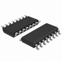
74HCT9046AD,118 NXP Semiconductors, 74HCT9046AD,118 Datasheet - Page 13

74HCT9046AD,118
Manufacturer Part Number
74HCT9046AD,118
Description
IC PLL BAND GAP CNTRL VCO 16SOIC
Manufacturer
NXP Semiconductors
Type
Phase Lock Loop (PLL)r
Series
74HCTr
Datasheet
1.74HCT9046AD118.pdf
(43 pages)
Specifications of 74HCT9046AD,118
Number Of Circuits
1
Package / Case
16-SOIC (3.9mm Width)
Pll
Yes
Input
Clock
Output
Clock
Ratio - Input:output
2:2
Differential - Input:output
No/No
Frequency - Max
16MHz
Divider/multiplier
No/No
Voltage - Supply
4.5 V ~ 5.5 V
Operating Temperature
-40°C ~ 125°C
Mounting Type
Surface Mount
Frequency-max
16MHz
Supply Voltage (max)
5.5 V
Supply Voltage (min)
4.5 V
Maximum Operating Temperature
+ 125 C
Minimum Operating Temperature
- 40 C
Mounting Style
SMD/SMT
Operating Supply Voltage
4.5 V to 5.5 V
Lead Free Status / RoHS Status
Lead free / RoHS Compliant
Lead Free Status / RoHS Status
Lead free / RoHS Compliant, Lead free / RoHS Compliant
Other names
568-1570-2
74HCT9046AD-T
935044180118
74HCT9046AD-T
935044180118
NXP Semiconductors
74HCT9046A_6
Product data sheet
Fig 12. Simple loop filter for PC2 without damping
R bias
I
17
cp
a. Simple loop filter for PC2
without damping
1
=
INPUT
R
----------- -
17
8.4 Loop filter component selection
bias
C2
C2
Using this equivalent resistance R3' for the filter design the voltage can now be expressed
as a transfer function of PC2; assuming ripple (f
Again this illustrates the supply voltage independent behavior of PC2.
Examples of PC2 combined with a passive filter are shown in
shows that PC2 with only a C2 filter behaves as a high-gain filter. For stability the damped
version of
Practical design values for R
to 15 k for the filter design. Higher values for R3' require lower values for the filter
capacitance which is very advantageous at low values of the loop natural frequency
K
I
cp
PC2
=
001aak449
OUTPUT
R3' C2
=
----- - V r
4
5
Figure 13
F
A
(j )
with series resistance R4 is preferred.
Rev. 06 — 15 September 2009
b. Amplitude characteristic
F
1/ A
j
bias
1
=
are between 25 k and 250 k with R3' = 1.5 k
---------------------------- -
1 A
+
1
j
001aak450
1
----------- -
j
r
1
= f
1
PLL with band gap controlled VCO
i
) is suppressed, as:
c. Pole zero diagram
Figure 12
A = DC gain limit, due to leakage
74HCT9046A
© NXP B.V. 2009. All rights reserved.
and 13.
001aak451
1/ A
1
Figure 12
13 of 43
n
.


