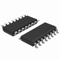
74HCT9046AD,118 NXP Semiconductors, 74HCT9046AD,118 Datasheet - Page 25

74HCT9046AD,118
Manufacturer Part Number
74HCT9046AD,118
Description
IC PLL BAND GAP CNTRL VCO 16SOIC
Manufacturer
NXP Semiconductors
Type
Phase Lock Loop (PLL)r
Series
74HCTr
Datasheet
1.74HCT9046AD118.pdf
(43 pages)
Specifications of 74HCT9046AD,118
Number Of Circuits
1
Package / Case
16-SOIC (3.9mm Width)
Pll
Yes
Input
Clock
Output
Clock
Ratio - Input:output
2:2
Differential - Input:output
No/No
Frequency - Max
16MHz
Divider/multiplier
No/No
Voltage - Supply
4.5 V ~ 5.5 V
Operating Temperature
-40°C ~ 125°C
Mounting Type
Surface Mount
Frequency-max
16MHz
Supply Voltage (max)
5.5 V
Supply Voltage (min)
4.5 V
Maximum Operating Temperature
+ 125 C
Minimum Operating Temperature
- 40 C
Mounting Style
SMD/SMT
Operating Supply Voltage
4.5 V to 5.5 V
Lead Free Status / RoHS Status
Lead free / RoHS Compliant
Lead Free Status / RoHS Status
Lead free / RoHS Compliant, Lead free / RoHS Compliant
Other names
568-1570-2
74HCT9046AD-T
935044180118
74HCT9046AD-T
935044180118
NXP Semiconductors
74HCT9046A_6
Product data sheet
Fig 24. Definition of VCO frequency linearity:
Fig 26. Power dissipation as a function of R1
(MHz)
10
10
(W)
P
f
D
f'
f
f
f
1
2
1
2
0
0
1
linearity =
0
R2 =
f‘
V = 0.5 V over the V
0
=
5.5 V
C1 = 1 F
4.5 V
C1 = 1 F
V
----------------- -
5.5 V
C1 = 39 pF
f
min
CC
1
4.5 V
C1 = 39 pF
+
2
f‘
----------------- -
=
0
f
f
2
100
–
0
f
V
0
0.5 V
100 %
CC
CC
range
200
V
R1 (k )
max
mbd121
V
mga937
VCO_IN
Rev. 06 — 15 September 2009
300
(V)
Fig 25. Frequency linearity as a function of R1, C1 and
Fig 27. Power dissipation as a function of R2
f
VCO
(%)
10
10
(W)
P
D
4
0
4
8
1
1
2
R2 =
V
0
R1 =
1
C1 = 1 F
4.5 V
5.5 V
CC
C1 =
39 pF
4.5 V
5.5 V
5.5 V
C1 = 39 pF
4.5 V
C1 = 39 pF
V
CC
5.5 V
4.5 V
C1 = 1 F
and V = 0.5 V
=
PLL with band gap controlled VCO
100
10
74HCT9046A
200
10
2
R2 (k )
© NXP B.V. 2009. All rights reserved.
R1 (k )
mbd114
mbd110
300
10
3
25 of 43


