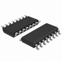
74HCT9046AD,118 NXP Semiconductors, 74HCT9046AD,118 Datasheet - Page 15

74HCT9046AD,118
Manufacturer Part Number
74HCT9046AD,118
Description
IC PLL BAND GAP CNTRL VCO 16SOIC
Manufacturer
NXP Semiconductors
Type
Phase Lock Loop (PLL)r
Series
74HCTr
Datasheet
1.74HCT9046AD118.pdf
(43 pages)
Specifications of 74HCT9046AD,118
Number Of Circuits
1
Package / Case
16-SOIC (3.9mm Width)
Pll
Yes
Input
Clock
Output
Clock
Ratio - Input:output
2:2
Differential - Input:output
No/No
Frequency - Max
16MHz
Divider/multiplier
No/No
Voltage - Supply
4.5 V ~ 5.5 V
Operating Temperature
-40°C ~ 125°C
Mounting Type
Surface Mount
Frequency-max
16MHz
Supply Voltage (max)
5.5 V
Supply Voltage (min)
4.5 V
Maximum Operating Temperature
+ 125 C
Minimum Operating Temperature
- 40 C
Mounting Style
SMD/SMT
Operating Supply Voltage
4.5 V to 5.5 V
Lead Free Status / RoHS Status
Lead free / RoHS Compliant
Lead Free Status / RoHS Status
Lead free / RoHS Compliant, Lead free / RoHS Compliant
Other names
568-1570-2
74HCT9046AD-T
935044180118
74HCT9046AD-T
935044180118
NXP Semiconductors
10. Recommended operating conditions
Table 4.
11. Static characteristics
Table 5.
At recommended operating conditions; voltages are referenced to GND (ground = 0 V).
74HCT9046A_6
Product data sheet
Symbol
V
V
V
T
Symbol
T
Phase comparator section
V
V
V
V
I
I
R
R
I
VCO section
V
V
I
OZ
cp
amb
t/ V
amb
CC
I
O
IH
IL
OH
OL
IH
IL
I
bias
= 25 C
Operating conditions
Static characteristics
Parameter
HIGH-level input voltage
LOW-level input voltage
HIGH-level output voltage
LOW-level output voltage
input leakage current
OFF-state output current
input resistance
bias resistance
charge pump current
HIGH-level input voltage
LOW-level input voltage
Parameter
supply voltage
input voltage
output voltage
ambient temperature
input transition rise and fall rate
Rev. 06 — 15 September 2009
Conditions
pins SIG_IN and COMP_IN;
V
pins SIG_IN and COMP_IN;
V
pins PCP_OUT and PCn_OUT;
V
pins PCP_OUT and PCn_OUT;
V
pins SIG_IN and COMP_IN;
V
pin PC2_OUT; V
V
SIG_IN and COMP_IN;
V
operating point; V
see
V
V
pin INH; V
DC coupled
pin INH; V
DC coupled
CC
CC
CC
CC
CC
I
CC
CC
CC
I
I
I
I
= V
O
O
O
O
Figure
= 4.5 V; DC coupled
= 4.5 V; DC coupled
= 4.5 V; V
= 4.5 V; V
= 5.5 V; V
= 4.5 V; V
= 4.5 V
= 4.5 V; R
= 20 A
= 4.0 mA
= 20 A
= 4.0 mA
IH
or V
Conditions
pin INH; V
CC
CC
14,
IL
= 4.5 V to 5.5 V;
= 4.5 V to 5.5 V;
; V
I
I
I
I
bias
15
= V
= V
= V
at self-bias
O
CC
and
= 40 k
= V
CC
IH
IH
CC
I
= 5.5 V;
= 0.5 V;
or V
or V
= 4.5 V
or GND
CC
16
or GND
IL
IL
PLL with band gap controlled VCO
Min
4.5
0
0
-
40
74HCT9046A
Min
3.15
-
4.4
3.98
-
-
-
-
-
25
2.0
-
0.53
Typ
5.0
-
-
1.67
Typ
2.4
2.1
4.5
4.32
0
0.15
-
-
250
-
1.6
1.2
1.06
© NXP B.V. 2009. All rights reserved.
Max
5.5
V
V
+125
139
CC
CC
Max
-
1.35
-
-
0.1
0.26
-
250
-
0.8
30
0.5
2.12 mA
Unit
V
V
V
ns/V
C
15 of 43
Unit
V
V
V
V
V
V
k
k
V
V
A
A


