ADF4213BCP Analog Devices Inc, ADF4213BCP Datasheet - Page 19
ADF4213BCP
Manufacturer Part Number
ADF4213BCP
Description
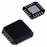
IC PLL FREQ SYNTHESIZER 20-LFCSP
Manufacturer
Analog Devices Inc
Type
Clock/Frequency Synthesizer (RF/IF)r
Datasheet
1.ADF4213BRU-REEL.pdf
(20 pages)
Specifications of ADF4213BCP
Rohs Status
RoHS non-compliant
Pll
Yes
Input
CMOS
Output
Clock
Number Of Circuits
1
Ratio - Input:output
3:1
Differential - Input:output
Yes/No
Frequency - Max
3GHz
Divider/multiplier
No/No
Voltage - Supply
2.7 V ~ 5.5 V
Operating Temperature
-40°C ~ 85°C
Mounting Type
Surface Mount
Package / Case
20-LFCSP
Frequency-max
3GHz
Available stocks
Company
Part Number
Manufacturer
Quantity
Price

Part Number:
ADF4213BCP
Manufacturer:
ADI/亚德诺
Quantity:
20 000


PCB Guidelines for Chip Scale Package
The lands on the chip scale package (CP-20), are rectangular.
The printed circuit board pad for these should be 0.1 mm
longer than the package land length and 0.05 mm wider than
the package land width. The land should be centered on the
pad. This will ensure that the solder joint size is maximized.
The bottom of the chip scale package has a central thermal pad.
The thermal pad on the printed circuit board should be at least
as large as this exposed pad. On the printed circuit board, there
should be clearance of at least 0.25 mm between the thermal
pad and inner edges of the pad pattern. This will ensure that
shorting is avoided.
0.035 (0.90) MAX
0.033 (0.85) NOM
INDICATOR
SEATING
PLANE
PIN 1
0.006 (0.15)
0.002 (0.05)
PIN 1
SEATING
12 MAX
PLANE
0.020 (0.50)
Thin Shrink Small Outline Package (TSSOP)
20
1
BSC
0.0256 (0.65)
0.157 (4.0)
BSC SQ
CONTROLLING DIMENSIONS ARE IN MILLIMETERS
0.260 (6.60)
0.252 (6.40)
VIEW
TOP
BSC
Dimensions shown in inches and (mm).
OUTLINE DIMENSIONS
0.031 (0.80) MAX
0.026 (0.65) NOM
0.008 (0.20)
0.0118 (0.30)
0.0075 (0.19)
REF
Chip Scale Package
0.148 (3.75)
0.0433 (1.10)
BSC SQ
11
10
MAX
0.177 (4.50)
0.169 (4.30)
(RU-20)
(CP-20)
0.0004 (0.01)
0.002 (0.05)
0.0 (0.0)
0.0035 (0.090)
0.0079 (0.20)
ADF4210/ADF4211/ADF4212/ADF4213
0.024 (0.60)
0.017 (0.42)
0.009 (0.24)
0.012 (0.30)
0.009 (0.23)
0.007 (0.18)
0.030 (0.75)
0.022 (0.60)
0.014 (0.50)
Thermal vias may be used on the printed circuit board thermal
pad to improve thermal performance of the package. If vias are
used, they should be incorporated in the thermal pad at 1.2 mm
grid pitch. The via diameter should be between 0.3 mm and
0.33 mm and the via barrel should be plated with 1 oz. copper
to plug the via. The user should connect the printed circuit
board pad to AGND.
0.256 (6.50)
0.246 (6.25)
0.024 (0.60)
0.017 (0.42)
0.009 (0.24)
8
0
15
11
10
16
0.080 (2.00)
BOTTOM
VIEW
REF
0.010 (0.25)
0.028 (0.70)
0.020 (0.50)
20
MIN
6
1
5
0.080 (2.25)
0.083 (2.10) SQ
0.077 (1.95)
Related parts for ADF4213BCP
Image
Part Number
Description
Manufacturer
Datasheet
Request
R

Part Number:
Description:
±1.7g Dual-Axis IMEMS Accelerometer Evaluation Board
Manufacturer:
Analog Devices Inc
Datasheet:

Part Number:
Description:
Inertial Sensor Evaluation System
Manufacturer:
Analog Devices Inc
Datasheet:
Part Number:
Description:
Manufacturer:
Analog Devices Inc
Datasheet:
Part Number:
Description:
Manufacturer:
Analog Devices Inc
Datasheet:
Part Number:
Description:
Manufacturer:
Analog Devices Inc
Datasheet:
Part Number:
Description:
Manufacturer:
Analog Devices Inc
Datasheet:
Part Number:
Description:
Manufacturer:
Analog Devices Inc
Datasheet:
Part Number:
Description:
Manufacturer:
Analog Devices Inc
Datasheet:
Part Number:
Description:
Manufacturer:
Analog Devices Inc
Datasheet:
Part Number:
Description:
Manufacturer:
Analog Devices Inc
Datasheet:
Part Number:
Description:
Manufacturer:
Analog Devices Inc
Datasheet:
Part Number:
Description:
Manufacturer:
Analog Devices Inc
Datasheet:
Part Number:
Description:
Manufacturer:
Analog Devices Inc
Datasheet: