ADF4213BCP Analog Devices Inc, ADF4213BCP Datasheet - Page 4
ADF4213BCP
Manufacturer Part Number
ADF4213BCP
Description
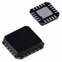
IC PLL FREQ SYNTHESIZER 20-LFCSP
Manufacturer
Analog Devices Inc
Type
Clock/Frequency Synthesizer (RF/IF)r
Datasheet
1.ADF4213BRU-REEL.pdf
(20 pages)
Specifications of ADF4213BCP
Rohs Status
RoHS non-compliant
Pll
Yes
Input
CMOS
Output
Clock
Number Of Circuits
1
Ratio - Input:output
3:1
Differential - Input:output
Yes/No
Frequency - Max
3GHz
Divider/multiplier
No/No
Voltage - Supply
2.7 V ~ 5.5 V
Operating Temperature
-40°C ~ 85°C
Mounting Type
Surface Mount
Package / Case
20-LFCSP
Frequency-max
3GHz
Available stocks
Company
Part Number
Manufacturer
Quantity
Price

Part Number:
ADF4213BCP
Manufacturer:
ADI/亚德诺
Quantity:
20 000


Model
ADF4210BRU
ADF4210BCP
ADF4211BRU
ADF4211BCP
ADF4212BRU
ADF4212BCP
ADF4213BRU
ADF4213BCP
ADF4210/ADF4211/ADF4212/ADF4213
TIMING CHARACTERISTICS
Parameter
t
t
t
t
t
t
NOTES
Guaranteed by design but not production tested.
Specifications subject to change without notice.
ABSOLUTE MAXIMUM RATINGS
(T
V
V
V
V
Digital I/O Voltage to GND . . . . . . –0.3 V to DV
Analog I/O Voltage to GND . . . . . . . . . –0.3 V to V
REF
IF
Operating Temperature Range
Storage Temperature Range . . . . . . . . . . . . –65°C to +150°C
Maximum Junction Temperature . . . . . . . . . . . . . . . . 150°C
TSSOP θ
CSP θ
CAUTION
ESD (electrostatic discharge) sensitive device. Electrostatic charges as high as 4000 V readily
accumulate on the human body and test equipment and can discharge without detection. Although
the ADF4210/ADF4211/ADF4212/ADF4213 features proprietary ESD protection circuitry, per-
manent damage may occur on devices subjected to high-energy electrostatic discharges. Therefore,
proper ESD precautions are recommended to avoid performance degradation or loss of functionality.
1
2
3
4
5
6
Contact the factory for chip availability.
DD
DD
P
P
A
Industrial (B Version) . . . . . . . . . . . . . . . . –40°C to +85°C
IN
1, V
1, V
= 25°C unless otherwise noted)
1 to GND
1 to V
A, IF
IN
JA
, RF
P
P
2 to GND . . . . . . . . . . . . . . . . . . . . . . –0.3 V to +7 V
2 to V
(Paddle Soldered) . . . . . . . . . . . . . . . . . . . 122°C/W
IN
JA
DD
IN
B to GND . . . . . . . . . . . . –0.3 V to VDD + 0.3 V
Thermal Impedance . . . . . . . . . . . . . 150.4°C/W
CLOCK
A, RF
2 . . . . . . . . . . . . . . . . . . . . . . . –0.3 V to +0.3 V
DATA
DD
3
LE
LE
1 . . . . . . . . . . . . . . . . . . . . –0.3 V to +5.5 V
. . . . . . . . . . . . . . . . . . . . . . . . –0.3 V to +7 V
Limit at
T
10
10
25
25
10
20
(B Version)
IN
MIN
B,
Temperature Range
–40°C to +85°C
–40°C to +85°C
–40°C to +85°C
–40°C to +85°C
–40°C to +85°C
–40°C to +85°C
–40°C to +85°C
–40°C to +85°C
to T
(MSB)
DB20
MAX
1, 2
Unit
ns min
ns min
ns min
ns min
ns min
ns min
t
1
(V
= AGND
DD
DB19
1 = V
IF
t
2
DD
= DGND
2 = 3 V
DD
P
ORDERING GUIDE
+ 0.3 V
+ 0.3 V
Package Description
Thin Shrink Small Outline Package (TSSOP)
Chip Scale Package
Thin Shrink Small Outline Package (TSSOP)
Chip Scale Package
Thin Shrink Small Outline Package (TSSOP)
Chip Scale Package
Thin Shrink Small Outline Package (TSSOP)
Chip Scale Package
IF
Test Conditions/Comments
DATA to CLOCK Hold Time
CLOCK High Duration
CLOCK Low Duration
CLOCK to LE Set-Up Time
LE Pulsewidth
DATA to CLOCK Set-Up Time
= 0 V; T
10%, 5 V
DB2
t
3
A
= T
CSP θ
Lead Temperature, Soldering
NOTES
1
2
3
TRANSISTOR COUNT
11749 (CMOS) and 522 (Bipolar).
Stresses above those listed under Absolute Maximum Ratings may cause perma-
This device is a high-performance RF integrated circuit with an ESD rating of
GND = AGND = DGND = 0 V.
nent damage to the device. This is a stress rating only; functional operation of the
device at these or any other conditions above those listed in the operational
sections of this specification is not implied. Exposure to absolute maximum rating
conditions for extended periods may affect device reliability.
< 2 kV and it is ESD sensitive. Proper precautions should be taken for handling
and assembly.
Vapor Phase (60 sec) . . . . . . . . . . . . . . . . . . . . . . . . 215°C
Infrared (15 sec) . . . . . . . . . . . . . . . . . . . . . . . . . . . . 220°C
MIN
10%; V
t
to T
4
JA
(CONTROL BIT C2)
(Paddle Not Soldered) . . . . . . . . . . . . . . . . 216°C/W
MAX
DD
unless otherwise noted.)
DB1
1, V
DD
2 ≤ V
P
1, V
P
2 ≤ 6 V
(CONTROL BIT C1)
DB0 (LSB)
WARNING!
t
5
10%; AGND
t
6
Package Option
RU-20
CP-20
RU-20
CP-20
RU-20
CP-20
RU-20
CP-20
ESD SENSITIVE DEVICE
RF
= DGND
RF
Related parts for ADF4213BCP
Image
Part Number
Description
Manufacturer
Datasheet
Request
R

Part Number:
Description:
±1.7g Dual-Axis IMEMS Accelerometer Evaluation Board
Manufacturer:
Analog Devices Inc
Datasheet:

Part Number:
Description:
Inertial Sensor Evaluation System
Manufacturer:
Analog Devices Inc
Datasheet:
Part Number:
Description:
Manufacturer:
Analog Devices Inc
Datasheet:
Part Number:
Description:
Manufacturer:
Analog Devices Inc
Datasheet:
Part Number:
Description:
Manufacturer:
Analog Devices Inc
Datasheet:
Part Number:
Description:
Manufacturer:
Analog Devices Inc
Datasheet:
Part Number:
Description:
Manufacturer:
Analog Devices Inc
Datasheet:
Part Number:
Description:
Manufacturer:
Analog Devices Inc
Datasheet:
Part Number:
Description:
Manufacturer:
Analog Devices Inc
Datasheet:
Part Number:
Description:
Manufacturer:
Analog Devices Inc
Datasheet:
Part Number:
Description:
Manufacturer:
Analog Devices Inc
Datasheet:
Part Number:
Description:
Manufacturer:
Analog Devices Inc
Datasheet:
Part Number:
Description:
Manufacturer:
Analog Devices Inc
Datasheet: